|
|||||||||||||
|
|
|||||||||||||
       |
Feature Articles: Quantum Cryptography Vol. 9, No. 9, pp. 43–47, Sept. 2011. https://doi.org/10.53829/ntr201109fa9 Superconducting Single-photon DetectorsAbstractThis article describes the fabrication and properties of a single-photon detector made of a superconducting NbN nanowire. It also discusses suitable materials for future high-performance detectors and describes new fabrication processes for MgB2 nanowire. 
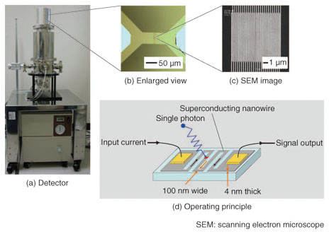
1. IntroductionQuantum cryptography is being intensively studied as a future optical network technology that assures the ultimate security in communications. In the standard optical communications network, one bit of information is represented by one optical pulse, which consists of more than 10,000 photons. In quantum cryptography, an extremely weak optical pulse consisting of less than one photon is used for one bit of information. It is impossible to amplify the optical pulse using an optical amplifier in a quantum cryptography network because quantum fluctuation, the essential feature of quantum cryptography, disappears with pulse amplification. The solution is to use high-performance single-photon detectors (SPDs) to increase the distance and speed of quantum cryptography communications. Many kinds of SPDs with different operating principles have been developed. Among them, SPDs made of a superconducting nanowire show the highest performance and are now used in many quantum cryptography experiments [1], [2]. 2. Superconducting SPDThe superconducting single-photon detector (SSPD) developed by NTT Basic Research Laboratories [3] is shown in Fig. 1. In general, superconducting devices need to be cooled to a very low temperature, and the complexity and large size of the liquid-helium cooling equipment often limits the practical application of superconducting devices. However, NTT's detector is only 110 cm × 50 cm × 60 cm in size and can fit into a standard 19-inch-wide rack. It uses a cryocooler, so one can reach below 3 K by simply switching on the 100-V AC supply. The superconducting device is located at the middle of the cylinder shown in Fig. 1(a). As shown in Figs. 1(b) and (c), it is 10 µm square. The nanowire inside the device is 100 nm wide and 4 nm thick (Fig. 1(d)). The device is illuminated by extremely weak optical pulses through an optical fiber from outside the cylinder.
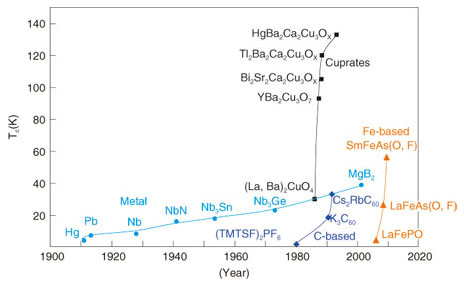
The mechanism of single-photon detection in the device is illustrated in Fig. 1(d). When electrical current flows in the superconducting nanowire, no voltage appears on the nanowire because the resistance is completely zero. When a single photon is absorbed at some point in the nanowire, the temperature at that point increases, superconductivity is locally de-stroyed, and the state at the point becomes normal (non-superconducting). If the nanowire is very narrow, the flowing current is completely protected by the normal state, and finite resistivity appears in the nanowire. Since the nanowire is being cooled by the cryocooler, its finite resistance rapidly disappears and it becomes superconducting again. These resistance changes create a voltage pulse, which is used to detect the arrival of a single photon at the superconducting nanowire. It may sound strange that only one photon can destroy superconductivity. However, while the superconducting energy gap of the superconductor is a few millielectron volts, the energy of a single photon at a wavelength of 1.5 µm is 0.83 eV, which is high enough to destroy superconductivity locally. From the above device operating principle, it is clear that the nanowire must be narrow enough to protect the superconducting current completely. This is achieved by using superconductor nanofabrication as fine as 100 nm and growth of an ultrathin superconducting film with a thickness of 4 nm. 3. Superconducting materialsAs the superconducting materials for the device, my colleagues and I used niobium (Nb) or niobium nitride (NbN) because they have well established nanofabrication and ultrathin film growth technologies. However, their transition temperatures (Tc) are relatively low among superconductors: 9 K for Nb and 16 K for NbN. Using a superconductor with a higher Tc would make it possible to operate the detector at a higher temperature, which would lead to further downsizing and energy savings. The discovery year and Tc of several superconductors are summarized in Fig. 2. Cuprates and iron- based superconductors seem to be good candidates for detectors because they have higher Tc values. However, these materials are complex compounds with four or more elements, so it is quite difficult to use them to fabricate high-quality ultrathin films and narrow nanowires with today's technologies [4].
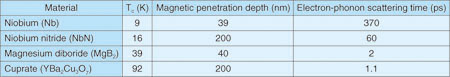
Magnesium diboride (MgB2) has a Tc of 39 K. This is lower than that of cuprate and Fe-based superconductors, but the highest Tc among metallic and inter-metallic compounds. MgB2 has a simple crystal structure with only two elements. Furthermore, device fabrication with MgB2 is not as difficult as that with cuprate and Fe-based superconductors. We can also expect faster operation with MgB2 than with Nb or NbN. Some physical superconducting parameters are listed in Table 1. The operating speed of an SSPD is governed by the inductance of the device and the electron-phonon relaxation time of the material. The inductance is determined by the device structure and by the material's magnetic penetration depth. For the same device structure, a device with a shallower magnetic penetration depth has a lower inductance and a faster response. On the other hand, a device with a shorter electron-phonon relaxation time has a faster response because it can rapidly return to the superconducting state again by emitting phonons. MgB2 has a shallower magnetic penetration depth and shorter electron-phonon relaxation time than NbN, so a device made of MgB2 operates faster than one made of NbN. The magnetic penetration depths of MgB2 and Nb are almost the same, but MgB2 has a much shorter electron-phonon relaxation time than Nb, so a device made of MgB2 also works faster than one made of Nb. The magnetic penetration depth of MgB2 is shallower than that of cuprate superconductors, but its electron-phonon relaxation time is longer. For devices with the same structure, one made of MgB2 operates faster than one made of cuprates. However, a cuprate-based device with an optimized structure would work faster than an optimally structured MgB2 device.
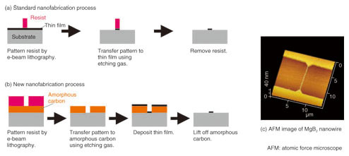
4. Fabrication of MgB2 nanowireAlthough MgB2 seems to be a promising material for high-performance SSPDs, technologies for ultrathin film growth and nanofabrication of MgB2 are not well established yet. We have succeeded in growing high-quality ultrathin MgB2 film by using molecular beam epitaxy (MBE), which lets us precisely control the evaporation rates of B and Mg independently. We have also developed a new MgB2 film nanofabrication technique. The standard nanofabrication process for thin films is illustrated in Fig. 3(a). The resist is spin-coated onto the film and patterned by electron beam lithography. Then the resist pattern is transferred to the thin film by etching. Finally, the resist is removed with an organic solvent and a nanopattern is obtained. The method can be applied to many kinds of materials if an appropriate etching gas is selected. It has been used to fabricate nanopatterns for many semiconductors including Nb and NbN. However, at present, it cannot be used for MgB2 because no etching gas for MgB2 has been found yet. Our new MgB2 film nanofabrication process is as follows (Fig. 3(b)). First, amorphous carbon is deposited on the substrate and resist is spin-coated onto the carbon film and patterned by electron beam lithography. Then the pattern is transferred to the amorphous carbon film by etching with a gas suitable for carbon (oxygen plasma). Next, the MgB2 film is deposited on the amorphous pattern by MBE. Finally, the amorphous carbon nanostructure is lifted off and the MgB2 nanopattern is obtained. The process is similar to the standard liftoff process using organic resist. However, the standard liftoff process does not work for MgB2 because the organic resist is destroyed by the high temperature used for MgB2 growth. By using inorganic amorphous carbon, we can grow MgB2 thin film at a high temperature without destroying the carbon nanopattern. An atomic force microscopy image of an MgB2 nanowire fabricated by our new method is shown in Fig. 3(c). The nanowire is smooth and 100 nm wide, 4 nm thick, and 10 µm long. Measurements of the superconducting properties of several nanowires confirmed that the electrical properties are not degraded during the nanofabrication process.
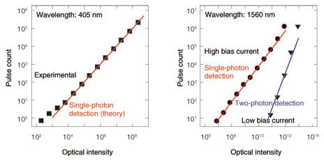
5. Single-photon-detection capability of MgB2 nanowireThe optical response of an MgB2 nanowire at different wavelengths is shown in Fig. 4. It is known that the number of photons in one optical pulse from an extremely weak coherent light source can be represented by the Poisson distribution function. In this case, the probability of detecting one photon is proportional to the mean photon number, which is equal to the optical intensity. Therefore, if the detector is capable of detecting a single photon, the number of electrical pulses from the detector should be proportional to the optical intensity. As shown in Fig. 4(a), this is indeed the case, which means that the detector can detect single photons having a wavelength of 405 nm. For a wavelength of 1560 nm, the number of electrical pulses is proportional to the square of the optical intensity in the low-bias region (Fig. 4(b)). This means that it is impossible to detect a single photon since the energy of a single 1560-nm photon is too weak. Therefore, two photons are necessary to generate an electrical pulse. In the high-bias region, on the other hand, the number of electrical pulses is proportional to the optical intensity, indicating that the MgB2 nanowire can have single-photon-detection capability even at 1560 nm. From these results, we conclude that the MgB2 nanowire has potential as a high-performance SPD.
6. ConclusionThe superconducting nanowire SPD that my colleagues and I have been using for quantum cryptography experiments is made of NbN. Toward practical quantum cryptography in future communications networks, we will continue to make efforts to improve the performance and reduce the energy consumption and size of detectors. A promising candidate for a high-performance SSPD is MgB2 nanowire. References
|
||||||||||||