|
|||||||||||||||||||||||||||||||||||
|
|
|||||||||||||||||||||||||||||||||||
       |
Regular Articles Vol. 10, No. 5, pp. 12–19, May 2012. https://doi.org/10.53829/ntr201205ra1 10-Gbit/s Phase-shift Keying Modulator and Demodulator MMICs for 120-GHz-band Wireless LinkAbstractWe are developing a 120-GHz-band 10-Gbit/s wireless link and have already demonstrated wireless transmission of a 10GbE (10 Gigabit Ethernet) data stream over a distance of 5.8 km. In its present state, the link uses amplitude shift keying (ASK) for the modulation scheme. To improve the system's performance, such as sensitivity and spectral efficiency, we need phase shift keying (PSK) modulation in the 120-GHz band. However, it is difficult to make a PSK modulator for frequencies above 100 GHz because the design is fundamentally more complicated than that for ASK. In this article, we introduce new PSK monolithic microwave integrated circuit technologies for 120-GHz-band 10-Gbit/s wireless links.
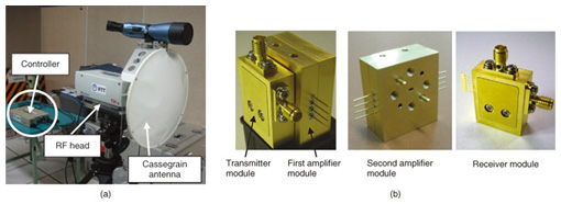
1. IntroductionThe capacity of data communication systems continues to increase each year to meet the data rates of high-speed protocols and those needed for the transfer of high-definition video. Along with this tendency, demand for high-speed wireless systems is also increasing. In the broadcasting field, standards for high-definition video, such as high-definition television (HDTV, 1.5 Gbit/s), three-dimensional video (3 Gbit/s), and 4K digital cinema (6 Gbit/s), have been developed to catch up with the demand for high-presence applications. To transmit them in a live-relay broadcast, broadcasting companies need a long-distance wireless technology that can handle multigigabit-per-second data streams. In communication networks, Gigabit Ethernet (GbE, 1 Gbit/s) and 10 Gigabit Ethernet (10GbE, 10 Gbit/s) have been widely used and the standard for the 10-Gbit/s Ethernet passive optical network (10G-EPON) was approved in 2009. Multigigabit-per-second wireless systems are useful for the last mile of fiber-to-the-home (FTTH) services and for setting up temporary connections to restore a network after a disaster or other disruptive event. To meet these demands, there has been a lot of interest in broadband wireless technologies using the millimeter-wave band from 30 to 300 GHz, because this band can provide sufficient bandwidth. In the 60-GHz band, some wireless systems that can transmit multigigabit-per-second data over a short distance have been reported [1], [2]. Some commercial point-to-point wireless links using 71–76 GHz and 81–86 GHz provide 1.25-Gbit/s data transmission over a link distance of more than 1 km. However, there are no practical wireless systems that can transmit 10-Gbit/s data a distance of 1 km. NTT Microsystem Integration Laboratories is developing a 10-Gbit/s wireless link [3] and monolithic microwave integrated circuits (MMICs) [4]. The wireless link will be suitable for fixed wireless access for 10GbE, OC-192, and certain other protocols. It will also be able to handle uncompressed high-definition video. There have already been several successful trials over distances of several kilometers; they include live relay broadcasts of HDTV [5], 10GbE transmissions in Sapporo, and 4K digital cinema streaming. At present, the link uses amplitude shift keying (ASK) and a bandwidth of 17 GHz for 10-Gbit/s data transmission with a spectral efficiency of 0.6 bit/s/Hz. In this article, we present 120-GHz-band wireless technologies that improve the link distance and spectral efficiency. First, we introduce the 120-GHz-band wireless link with ASK modulation and transmission experiments over a distance of 5.8 km [6]. The transmitter’s output power was increased by a power amplifier module having a high-breakdown-voltage high electron mobility transistor (HEMT) [7]. Second, we describe 10-Gbit/s phase shift keying (PSK) modulation technologies in the 120-GHz band. We explain the design of new binary PSK (BPSK) and quadrature PSK (QPSK) modulator MMICs [8], [9] in the 120-GHz band and present 10-Gbit/s data transmission characteristics of BPSK and QPSK modules. 2. Configuration and field experienceA photograph of a 120-GHz-band wireless link with the ASK modulation scheme is shown in Fig. 1(a). The wireless transmitter was designed to have usability and configuration equivalent to the field pick-up unit currently in wide use by broadcasters. The transmitter head generates a 125-GHz signal as a radio-frequency (RF) carrier, modulates it with a 10-Gbit/s baseband signal, and amplifies the modulated signal to 16 dBm. The receiver head receives the incoming signal, amplifies it using a low-noise amplifier (LNA), and demodulates 10-Gbit/s data. The controller supplies power, the data signal, and control signals to the head. The antenna used by the wireless link is chosen from four available kinds: three Cassegrain antennas with diameters ranging from 100 mm (gain: 37 dBi) to 600 mm (gain: 52 dBi) and a standard horn antenna with gain of 23 dBi. Photographs of RF modules for generating, modulating, amplifying, and demodulating the millimeter-wave signal are shown in Fig. 1(b). The transmitter module, the first amplifier module, and the receiver module use indium-phosphide (InP HEMT MMICs) developed by NTT Photonics Laboratories. The second power amplifier module uses 0.08-μm-gate-length InGaAs/InP HEMT MMICs, which have higher breakdown voltages. The on- and off-state breakdown voltages are around 4 V and 10 V, respectively. These values are almost double those of conventional InP HEMTs. The devices typically have current-gain cut-off frequency fT of 180 GHz and a maximum oscillation frequency fmax of 650 GHz. The second power amplifier with composite-channel HEMTs has demonstrated maximum output power of 140 mW and output P1dB of 80 mW at 125 GHz [7].
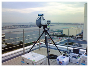
We conducted field transmission experiments using the 120-GHz-band wireless link shown in Fig. 2. The data rate was 10.3125 Gbit/s (forward error correction rate: 11.1 Gbit/s) and the transmission distance was 5.8 km in the fine weather during the experiments. The transmitter and receiver antenna gains were 52 dBi and 49 dBi, respectively. The 120-GHz-band wireless link performed error free transmission (bit error rate (BER): less than 10-12) during the experiment. At present, that is the longest reported distance for 10-Gbit/s wireless transmission.
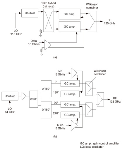
3. PSK MMICs technologiesOur current link uses the ASK modulation scheme; this is the simplest architecture, but it has poor spectral efficiency because it uses binary modulation and it has lower sensitivity than other binary modulation schemes. We need a different modulation scheme with greater sensitivity and better spectral efficiency in order to extend the transmission distance or reduce the occupied bandwidth. For that purpose, PSK is promising. BPSK modulation, which uses two phases which are separated by 180°, has the highest sensitivity among binary modulation schemes so it enables a longer link distance for 120-GHz wireless transmission. QPSK uses four phases and can encode two bits per symbol. QPSK has double the spectral efficiency of ASK for the same bitrate because it is a higher-order modulation. It lets us use the 120-GHz-band 10-Gbit/s wireless link with less occupied bandwidth or increase the capacity of the same occupied bandwidth. The design of a PSK demodulator is more complicated than that of an ASK modulator owing to the need for a phase-comparison circuit. In this section, we present PSK modulator and demodulator MMICs for 10-Gbit/s data transmission in the 120-GHz band. Two system requirements for a 120-GHz-band wireless link are the ability to handle 10-Gbit/s data with the same BER performance as the ASK system and to have a simple architecture. The ASK used for our wireless link has the advantage of a very simple architecture, which enabled us to design the ASK modulator and demodulator in a small area and integrate each one into an MMIC with other circuits on one chip. This is an advantage for reducing the fabrication cost of MMICs. To make the architecture of PSK MMICs simple, we chose differentially coherent detection for PSK demodulation since the differentially coherent detector does not need carrier-recovery circuits. In addition, we designed the modulator and demodulator without intermediate-frequency circuits. The total size of these circuits should be smaller than those that do have intermediate-frequency circuits, which makes it possible to implement them in a small area. The design goal is to make an integrated one-chip BPSK modulator and an integrated one-chip BPSK demodulator. 3.1 PSK modulator MMICBlock diagrams of the BPSK and QPSK modulator MMICs are shown in Figs. 3(a) and (b), respectively. To implement direct modulation, we chose a simple architecture consisting of 90º and 180º hybrid couplers, switches, and combiners. The gain-control amplifier (GC amplifier) acts as an on-off switch according to the applied voltage level. When the level is high, a signal fed into the GC amplifier is amplified by 10 dB; when the level is low, the signal is attenuated by more than 20 dB, resulting in a 30-dB on-off ratio. The Wilkinson combiner combines the output signals of the GC amplifiers. For BPSK, when the voltage level is high (corresponding to a data bit value of 1), the GC amplifiers amplify the 0º signal and when it is low (corresponding to a bit value of 0), they amplify the 180º signal. For QPSK, when (I, Q) is (1, 1), the GC amplifiers for the I (in-phase) channel amplify the 0º signal, and the GC amplifiers for the Q (quadrature) channel amplify the 90º signal. The phase of the combined RF signals therefore becomes 45º. To decrease the required frequency of the modulator MMIC, we used a doubler circuit, which converts the local signal to the carrier signal. This reduces insertion loss generated at wire-bonding sites. We also designed a differential amplifier to control the GC amplifiers. The differential amplifier divides input data into positive and negative data values and shifts the voltage levels to appropriate values for GC amplifiers.
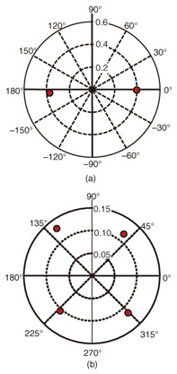
We evaluated the magnitude of the static error vector of the designed modulators. The S21 characteristics of the BPSK and QPSK modulator MMICs are shown in Fig. 4. S21 of the BPSK modulator MMIC had the maximum phase error of 5° and amplitude error of 3% when DC voltages were applied. These errors mainly come from the characteristics of the rat-race circuit. From these values, we estimated the static error vector magnitude to be about 5%. For QPSK, S21 for phases of 45º, 135º, 225º, and 315º had a maximum phase error of 8º and maximum amplitude error of 11%. From these values, we obtained a static error vector magnitude of about 10%.
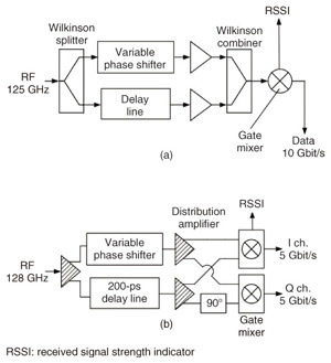
3.2 PSK demodulator MMICBlock diagrams of the BPSK and QPSK demodulator MMICs are shown in Fig. 5. As mentioned in section 3, we selected differentially coherent detection because it has a simple architecture and does not require carrier-recovery circuits. First, the received signal is split into two. One part is delayed by the length of a data symbol. The other part goes through a variable phase shifter. The two signals are combined and mixed by a gate mixer. The main issues in this architecture are the design of the one-symbol delay circuit and control of the phase relationship between the two split signals. In our delay circuit design, the delay line is basically made of a transmission line; this provides an accurate delay time but has the drawback of being very long. The modulators using BPSK and QPSK need to be about 13 mm and 25 mm, respectively, if the delay line consists of only a coplanar waveguide with a width of 15 μm and space of 15 μm. To reduce the length, we made the delay line by alternating metal-insulator-metal shunt capacitors and coplanar waveguides. As a result, the actual lengths of our delay lines for BPSK and QPSK are 5 mm and 10 mm, respectively. Next, we designed a variable phase shifter to adjust the phase relationship between the received and delayed signals prior to mixing. The variable phase shifter consists of coplanar waveguides and cold field effect transistors, which are HEMTs. This circuit can adjust the electrical length continuously by changing the capacitances of the parasitic capacitors of the HEMTs. Thus, we can tune the phase of the output signal by means of an applied voltage. The designed tuning range of this circuit is over 180° at 125 GHz, which makes it possible to respond to any phase error caused by variations in process, voltage, or temperature.
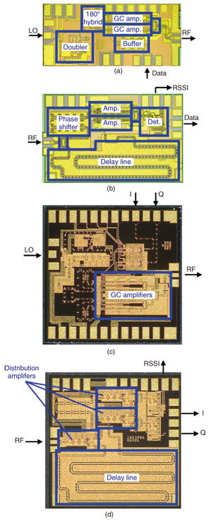
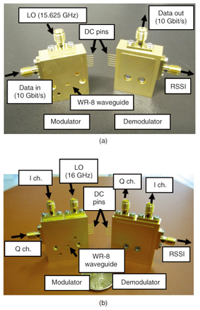
3.3 Evaluation for 10-Gbit/s data transmissionWe used 0.1-μm-HEMT technology on an InP substrate. The devices have a current-gain cut-off frequency (fT) of 170 GHz and a maximum oscillation frequency (fmax) of 350 GHz. Photographs of the modulator and demodulator MMICs are shown in Fig. 6. We succeeded in making a one-chip BPSK modulator and a one-chip BPSK demodulator. Before measuring the BERs, we mounted the modulator and demodulator MMICs in separate packages, as shown in Fig. 7. Thanks to the one-chip integration of the modulator and demodulator circuits, we obtained compact modulator and demodulator modules. The package has a WR-8 waveguide for the 120-GHz-band RF signal interface. Transitions from a rectangular waveguide to a coplanar waveguide were needed to transfer the RF energy from the coplanar waveguide to the WR-8 waveguide and vice versa.
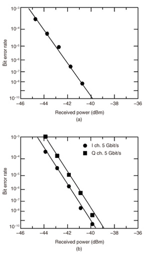
We then measured the BER of 10-Gbit/s data transmission. To measure the minimum received power, we set an LNA [10] in front of each demodulator module. The MMIC in the LNA module was the same as that used for our current ASK-based wireless link, and the noise figure was 5.6 dB. For delay detection, input data for the modulator module usually goes through a Gray-code adder, which has a one-symbol delay circuit. In this measurement, a pulse pattern generator directly outputs the data encoded by the Gray-code adder. In addition, a limit amplifier for 10-Gbit/s base-band signals was installed after the demodulator module to satisfy the required power for the error detector. The relationship between the LNA’s received power and the measured BER is shown in Fig. 8. BPSK and QPSK modules achieved a BER of less than 10-10 at received power of -39.5 dBm and -38.5 dBm, respectively. In the current ASK-based link, the received power at a BER of 10-10 is -38.5 dBm. If we simply compare these values, it would appear that we can indeed make BPSK and QPSK systems with the same transmission performance with the ASK system. However, in this measurement, some conditions were different from those for the ASK system. For example, there was no RF filter at the demodulator and no power amplifier for the modulator. It is possible that using an RF filter in the demodulator will further improve the sensitivity.
Finally, we estimated the transmission distance of the 120-GHz-band wireless link with 10-Gbit/s BPSK and QPSK. To make the link, we need additional RF components, i.e., power amplifiers, antennas, and RF filters. For this purpose, we can use the same amplifiers and antennas as those for the ASK-based wireless link [3] because the operating band for ASK covers those for BPSK and QPSK. By using such amplifiers, we should obtain output power of 10 dBm. Moreover, the antenna gains of the transmitter and receiver are both 48.7 dBi. The relationship between link distance and other characteristics is as follows: 4. Future plansWe hope to implement BPSK and QPSK modules in the 120-GHz-band wireless link. We would also like to improve the analysis of the propagation characteristics of 120-GHz-band millimeter-wave signals, especially their dependency on weather, by making use of data from long-term, continuous transmission tests. AcknowledgmentsThis research was partially done under contract with the Ministry of Internal Affairs and Communications under the “RF Resource Use R&D” initiative. References
|
||||||||||||||||||||||||||||||||||