|
|||||||||||||||||||||||||||||||||||||||||||||||||||||||||||||||||||||||||||||||||
|
|
|||||||||||||||||||||||||||||||||||||||||||||||||||||||||||||||||||||||||||||||||
       |
Regular Articles Vol. 11, No. 5, pp. 25–36, May 2013. https://doi.org/10.53829/ntr201305ra1 Historical Overview of Semiconductor Device Reliability for Telecommunication Networks––
|
||||||||||||||||||||||||||||||||||||||||||||||||||||||||||||||||||||||||||||||||
 |
 |
1. Introduction
From the 1960s to the 1980s, NTT’s use of semiconductor devices was the primary factor in the successful development of highly reliable and miniaturized high-performance telecommunications equipment. In the 1960s, the semiconductor industry was in its infancy. Therefore, it was not really known how reliable semiconductor devices would be, and experience in using them in telecommunications equipment was lacking. At that time, NTT was the first company in the world to introduce transistors into telecommunications equipment [1]–[7].
In the early 1960s, NTT introduced a failure physics approach (also known as the physics of failure), described in the next section, in order to develop highly reliable semiconductor devices for telecommunications equipment. The target values for device reliability required in network system design were a lifetime longer than 25 years and a failure rate lower than 0.2–150 FIT (failure in time, which is defined as the number of failures per billion device hours (10-9/h)), depending on the type of device (from diodes to LSIs (large-scale integrated circuits)) and the kind of equipment [4]. For semiconductor devices that had been developed at that time, accelerated life tests (longer than 10,000 hours) and long-term operation tests at room temperature using a large number of devices were conducted to confirm that those targets had been achieved. In addition, field failure tests were carried out with actual working equipment to confirm the high reliability of semiconductor devices and of passive and mechanical components as well.
On the basis of the results of those field failure tests, we developed a failure rate prediction model for electronic components including semiconductor devices to use in the reliability design of the next stage of our telecommunications equipment [8], [9]. The objectives of this failure rate prediction model were the same as those of the well-known MIL-HDBK-217 (Military Handbook) model for reliability prediction of electronic equipment [10], and the procedures were similar.
The development of reliability assurance standards such as MIL-STD (Military Standard) -19500 [11] and MIL-STD-38510 [12] started in the late 1950s, and NTT applied them to semiconductor devices installed in NTT equipment to ensure their high reliability [8]. Over the years, NTT also developed and periodically revised its own assurance standards to reflect advances in device technology. These standards were finally withdrawn in 1987 because the reliability of semiconductor devices had been improved to the level where such standards were no longer necessary.
2. Development of highly reliable devices based on the failure physics approach
The failure physics approach for developing highly reliable devices is as follows; first, various failure modes are investigated in accelerated life tests. Next, associated failure mechanisms are clarified, and device reliability is improved by optimizing device structures and fabrication processes. Finally, a reliability assurance procedure is carried out; this procedure includes conducting wafer acceptance tests, screening tests of encapsulated devices for eliminating early failures, and lot-acceptance tests.
The procedure we followed for developing highly reliable semiconductor devices is shown in Fig. 1, and examples of devices used in NTT equipment are summarized in Table 1 [13], [14]. The relationship between failure rate and working time is known as the bathtub curve, which depicts the early failure period, random failure period, and wear-out failure period. Early failures are caused by latent defects induced during fabrication, and the failure rate decreases with time (β < 1, where β is the shape parameter in a Weibull distribution). Random failures are caused by small latent defects that occur after relatively long-term operation at a constant failure rate (β = 1). Wear-out failures occur after long-term operation due to wear-out and fatigue, and the failure rate tends to increase rapidly during this period (β > 1).
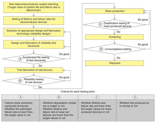
Fig. 1. Procedure for developing highly reliable semiconductor devices for telecommunications equipment.
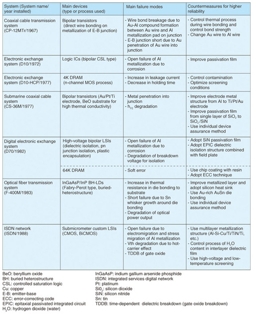
Table 1. Main devices used in various telecommunication systems, failure modes, and countermeasures for higher reliability.
Countermeasures consisting of fabrication process control and proper screening were effective in reducing the failure rate of early failures. For random failures, long-term tests conducted under actual working conditions confirmed that failure rates were lower than the target value. Wear-out failures, which should never occur during the guaranteed lifetime of a device, were prominent for miniaturized LSIs and optical devices. These failures are classified into degradation-related failures and catastrophic ones. Examples of degradation failures are a decrease in the optical output power of laser diodes (LDs) or changes in the current gain (hFE) of bipolar transistors during operation. In a circuit affected by such degradation, the extent of the degradation has to be accurately estimated in order to analyze its effect on circuit operation in the intended working conditions. Examples of catastrophic failures are the lifting of Au (gold) wire bonding and stressmigration in Al (aluminium) interconnections in plastic-encapsulated LSIs. Wear-out failure analyses that we performed for plastic encapsulated LSIs and LDs are described in more detail in section 4.
3. Failure rate in field use and reliability prediction model
3.1 Failure rate data in field use
From the 1960s to the 1980s, NTT collected a large amount of data on field failures of devices in NTT telecommunications equipment. The devices were typically operated in an air-conditioned room with a maximum junction temperature of 55ºC (ambient temperature 40ºC) and relative humidity of 20–70% [5], [15]–[25].
The relationships between the failure rate of devices (in failures/109 hours = FIT) in field use and the installation year for diodes, bipolar transistors, and bipolar integrated circuits (ICs) are shown in Fig. 2. These values were selected from field data of more than 1×10¹⁰ device·hours for diodes, 4×10⁹ device·hours for bipolar transistors, and 5×10⁸ device·hours for bipolar ICs, which corresponded to one to three years of operation. The lower limits of the failure rate estimation are 0.01 FIT for diodes, 0.25 FIT for transistors, and 2 FIT for bipolar ICs. These lower limits are one order lower than the observed failure rate as described below.
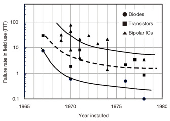
Fig. 2. Failure rate in field use vs. year installed in NTT equipment for semiconductor devices.
As shown in Fig. 2, the failure rate decreased with time and approached a certain constant value depending on the device group. These curves are similar to the so-called learning curve, and the constant value corresponds to the failure rate in the random failure period for mature devices. The failure rate seemed to become higher as the process complexity increased. The failure rate in the random failure period was estimated to be about 0.2 FIT for diodes, about 2 FIT for transistors, and about 5 FIT for bipolar ICs. The failure rate observed in field use from the 1960s to the 1980s for more precisely divided device groups in the random failure period is plotted in Fig. 3. The figure shows that somewhat high failure rates were observed for metal-oxide semiconductor (MOS) ICs, which had just been developed and had not yet matured in those days, though the failure rates were less than 100 FIT. We also examined the failure rate for LSIs developed in the 1990s by conducting accelerated life tests with a large number of LSIs for about 3000 hours. We found that the failure rates of memory LSIs such as 64-K–1-M DRAM (dynamic random access memory) were below 100 FIT, and those of CMOS (complementary MOS) logic LSIs (about 150-K gates) fabricated with 0.25–0.5 µm technology were below 200 FIT. The failure rates of these LSIs were expected to decrease in the accelerated life tests and approach a constant value below 100 FIT if the tests were continued beyond 3000 hours, because no failures were observed within the first 3000 hours.
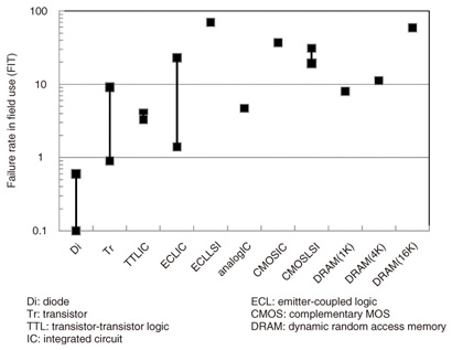
Fig. 3. Failure rate in field use in random failure period for various semiconductor devices.
3.2 Failure rate prediction models
3.2.1 NTT model
A failure rate prediction model was developed on the basis of the collected field data and used in the next stage of equipment design [8], [9], [26], [27]. The NTT failure rate prediction model (called the NTT model hereafter) was sought to determine the constant failure rates in the random failure period and was similar to the well-known MIL-HDBK-217 model. It was established for semiconductor devices and passive and mechanical components used for NTT equipment. The failure rate of ICs is expressed as
where λ is the predicted failure rate, λb is the basic failure rate (FIT), πQ is the quality factor, πE is the environmental factor, πT is the temperature factor, and πV is the power supply voltage factor.
The basic failure rate λb was defined for each device type, integration level, and technology. For example, the λb of bipolar digital logic ICs and MOS DRAM is listed in Table 2.
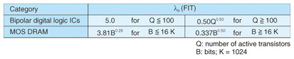
Table 2. Example of basic failure rate of ICs.
Quality factor πQ was given a value from 1 to 4, depending on the quality grade defined by NTT; it was 1 for highly reliable ICs (namely, quality-controlled devices used in NTT equipment). Environmental factor πE was given a value from 0.3 to 1.8, depending on the operating environment such as an air-conditioned room, vehicle, or mobile telephone; it was 0.3 for an air-conditioned room. Power supply voltage factor πV was expressed as πV = 0.35 × exp (0.21VDD) for CMOS ICs and 1 for other devices.
Temperature factor πT is given as
where k is Boltzmann’s constant and Tj is junction temperature at the operating condition. This formula was derived by considering the contribution to the failure of two activation energies (Ea) of 0.3 and 0.7 eV. Here, various failure mechanisms showed different activation energies, and the major failure mechanisms for MOS ICs were gate oxide breakdown (TDDB) with Ea=0.3 eV and electromigration or stressmigration of metallization with Ea=0.7 eV. Activation energies for these major failure mechanisms were therefore introduced to define the temperature factor in the NTT model.
Unlike the MIL-HDBK-217 model, the NTT model considered the effect of packaging only for hermetic or non-hermetic (plastic-encapsulated) sealing and did not take the effect of package type or size into account.
3.2.2 Comparison of NTT model with other failure rate prediction models
The final revised version of the NTT model was completed in 1981 and published in 1982 [8]. In those days, comparable prediction models for electronic components were MIL-HDBK-217 (version C (1979) and version D (1982)), and Bellcore TR-332 [28]. Later, other failure rate prediction models were developed such as PRISM [29] and IEC/TR (International Electrotechnical Commission/Technical Report) 62380 [30]. These models consider not only individual components but also the total system operation, and they differ from device-oriented models such as the NTT model and MIL-HDBK-217. Quantitative comparisons of the predicted trend of failure rates among these various models were needed but had not been carried out [31], [32]. We therefore performed comparisons between six device-oriented models of the NTT model (1981), three versions of the MIL-HDBK-217 model (C(1979), E(1986), F(1991)), and two versions of the Bellcore model (TR-332 issue (1997), SR-332 issue 2 (2006)). (Note that TR-332 was changed to SR-332 in 2001.) Operating conditions were assumed to be Tj = 55ºC (ambient temperature of 40ºC) and an air-conditioned room, which corresponded to “Ground, Benign” in MIL and also to the NTT electronic switching system environment. The quality grade was selected as the highest reliable level at NTT, i.e., πQ = 1, which was equivalent to MIL-class B. The power supply voltage factor was a standard voltage, and πV = 1. Under these conditions, comparisons of failure rate were performed for NMOS (n-channel MOS) DRAM and bipolar digital logic ICs as a function of the scale of integration. The results are shown in Figs. 4 and 5.
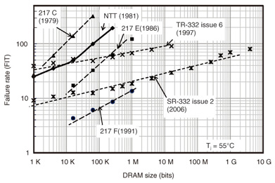
Fig. 4. Predicted failure rate vs. size of DRAM for various failure rate prediction models.
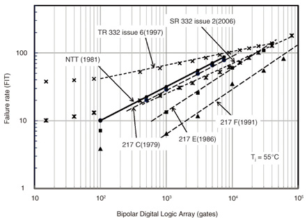
Fig. 5. Predicted failure rate vs. number of gates in bipolar logic IC gate arrays for various models.
For DRAM, the failure rate prediction curve obtained with the NTT model lies between MIL-HDBK-217 C(1979) and 217 E(1986), and the relationship between failure rate and DRAM size seems to shift in parallel with subsequent versions, i.e., the year of publication. For digital logic ICs, the prediction curves tend to converge at around 200 FIT with increases in the number of gates, regardless of the model. The features of the relationship between failure rate and scale for DRAM are somewhat different from those for bipolar logic ICs. This difference can be explained as follows; the process technology for DRAM had been revised with the very large scale production more quickly than it had for bipolar logic ICs. Consequently, the yield and reliability were improved more quickly compared with bipolar digital ICs. The trend in the predicted results indicated that the failure rate of LSIs would converge to a constant value regardless of the scale of integration, and that value was estimated to be 100–200 FIT even for the maximum scale of integration for a given year. On the whole, the relationship between failure rate and scale of integration can be assumed to shift in parallel with the fabrication year due to advances in technology. Although these prediction models involving the NTT model are old, they can still be used as references for predicting failure rates of recently developed devices.
4. Examples of analyses for wear-out failure modes
Wear-out failure is divided into catastrophic failure and degradation failure modes, as mentioned previously. The time to reach wear-out failures has tended to decrease with the rapid progress in the miniaturization of device dimensions used in LSIs since the latter half of the 1980s. Reliability analyses of plastic-encapsulated LSIs and LDs are described below as respective examples of catastrophic and degradation failures.
4.1 Reliability analysis for catastrophic failures
A reliability analysis was carried out for plastic-encapsulated MOS DRAMs, in which typical failure modes were open failures caused by the lifting of Au wire-bonds and stressmigration of Al(Si) metallization [13]. Weibull plots of failures observed in high-temperature operating tests for 64-K, 256-K, and 1-M DRAMs are shown in Fig. 6. Failure analyses clarified that the failures involved the lifting of Au wire-bonds for the 64-K and 256-K DRAM and stressmigration of Al(Si) metallization for the 1-M DRAM. Au wire-bond failures were induced by thermal expansion mismatch among the molding compounds (10–20 ppm/ºC), Au wire (14 ppm/ºC), and Si (3 ppm/ºC), and also by decreases in the thermal expansion coefficient of molding compounds during high-temperature aging. Stressmigration failure was caused by tensile stress due to the thermal expansion difference between the Al interconnection and the intermediate layer.
.jpg)
.jpg)
Fig. 6. (a) Failures observed for plastic encapsulated DRAM in high-temperature operation tests and (b) estimated failure rate vs. time under normal operating temperature (Tj = 55ºC).
Weibull parameters determined from the results of the accelerated life tests shown in Fig. 6(a) are listed in Table 3. The values of the shape parameter β were 6.5 for 64-K and 256-K DRAM and 2.5 for 1-M DRAM, which indicates the wear-out failures. The activation energy of the Au wire-bond open failure was estimated to be 1.25 eV for 64-K DRAM, and was assumed to be the same for the 256-K DRAM. The activation energy of the Al(Si) stressmigration failure observed in the 1-M DRAM in the 150ºC and 175ºC tests was estimated to be 0.15 eV. However, the failure rate for stressmigration was known to have a plateau around 180ºC and to show complicated temperature dependence [33]. Therefore, 0.55 eV was adopted as the activation energy for failure rate estimation, in which the energy was derived from testing below 150ºC using other test structures [34].
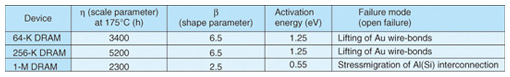
Table 3. Weibull parameters determined from high-temperature operation tests for NMOS DRAM.
The relationship between estimated failure rate and operating time at the operating temperature of 55ºC derived from the above parameters is shown in Fig. 6(b) in a Weibull distribution. Here, the failure rate in the Weibull distribution was obtained by
The target value of the failure rate for catastrophic wear-out failures was set at 10 FIT after 25 years. The failure rates of 64-K and 256-K DRAM were far below the target value, while that of the 1-M DRAM reached the target value after only one year, as shown in Fig. 6(b), which indicates an obvious need for improvement. The1-M DRAM was subsequently improved by using Al(Si, Cu) interconnections instead of Al(Si) interconnections, and the lifetime of the improved 1-M DRAM was confirmed to be 100 times longer than the former one.
Further, room-temperature operating tests were carried out over 17,400 hours with 320 samples, and the results confirmed that the rates of random failures of 64-K DRAM were below 165 FIT. For the 1-M DRAM, 150ºC operating tests using 110 samples for a duration of 10,000 hours confirmed that the rates of random failures were below 62 FIT. The analyses of wear-out failures and random failures confirmed that the total failure rates satisfied the target values.
4.2 Reliability analysis for degradation failures
Degradation of electrical characteristics is a major concern for semiconductor devices such as LDs, whose optical output power degrades with time. Degradation analyses, therefore, are needed in addition to random failure examination and are typically obtained by conducting accelerated life tests. It is imperative to confirm that the amount of degradation during the guaranteed duration of use is within the designated value by analyzing the degradation characteristics. A reliability analysis was done to determine the characteristic degradation of LDs used in the FS-400M submarine optical telecommunications system.
Samples were Fabry-Perot buried type InGaAsP-LDs with a 1.3 μm wavelength. In actual applications, an automatic power control (APC) circuit was used to maintain a constant optical output power; i.e., degradation of the constant output power of LDs was maintained by the increase in driving current in the APC circuit. The failure criterion of the LD degradation was normally defined by a 50% increase in driving current. The accelerated life tests were conducted in conditions of 50ºC and 70ºC temperatures with an output power of 5 mW, and also at 10ºC and 5 mW, which was the actual operating condition. In total, 1000 samples were tested, with 100 samples used for the 10ºC test, 800 samples for the 50ºC test, and 100 samples for the 70ºC test. The rate of random failures was also estimated by testing the same 1000 samples [35].
4.2.1 Degradation mode of electrical characteristics
The degradation mode was a decrease in optical output power, and the degradation corresponded to an increase in the driving current in the APC circuit, which could be easily monitored. The typical degradation characteristics in the 70ºC test are shown in Fig. 7. The driving current increased with time as ΔId/Io (t) ∝tn, where ΔId is the increase in driving current, Io is the initial driving current, t is the test time, and n is a constant. The value of n varied with the samples in the range of 0.4–1.0. The lifetime, which is defined as the time to reach a 50% increase in driving current, was estimated by extrapolating the relation shown in Fig. 7 for each sample. A log-normal plot of cumulative failures versus lifetime for the 70ºC operating test is shown in Fig. 8(a). This log-normal distribution was approximated by the median life of µ = 1.4 × 10⁵ hours and the standard deviation of σ = 0.99, except for the long lifetime portion. Although the activation energy was estimated to be about 0.8 eV from the data at 50ºC and 70ºC, the lowest activation energy of 0.35 eV used in semiconductor devices was applied in order to obtain a more severe prediction in the actual lifetime estimation. The failure rate is given by the following equation for the log-normal distribution [36]:
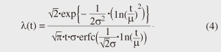
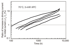
Fig. 7. Driving current degradation of LDs used in FS-400M system during high-temperature operating test.
.jpg)
.jpg)
Fig. 8. (a) Lifetime distribution of LDs derived from Fig. 7 and (b) failure rate prediction at 10ºC (failure criterion is 50% increase in driving current).
The estimation of failure rate versus time (years) at 10ºC in the actual undersea environment is shown in Fig. 8(b). From this plot, a failure rate of 220 FIT after 25 years was estimated, while 0.001 FIT after 25 years was estimated when 0.8-eV activation energy was applied.
4.2.2 Random failure mode
Long-term reliability testing for 19,000 hours at maximum was carried out for 1000 samples as described above. Except for optical output degradation, no catastrophic failures were observed in these tests. A failure rate lower than 13 FIT (CL=60%) was estimated from these tests of 7.3 × 10⁷ device·hours at 10ºC, where 0.35-eV activation energy was used. Thus, the total rate of wear-out failure and random failure was estimated to be below 233 FIT, which was below the target value of 300 FIT at 10ºC operation and 25 years duration.
4.2.3 Screening
The operating test results showed a relatively good correlation between the increase in driving current at 1000 hours and the lifetime estimated using the procedure described above with a correlation coefficient of -0.62. This indicates that a failure rate one order of magnitude lower than 300 FIT could be obtained by selecting LDs with a smaller increase in driving current after 1000 hours of aging. This procedure was implemented as the third step of screening, where the total screening consisted of three steps: 70ºC/150 mA for 100 h, 70ºC/8 mW with APC for 100 h, and 70ºC/5 mW with APC for 1000 h [35]. The first and second steps were used to avoid early failures and stabilize the electrical characteristics, and the third step was done to select a long-lifetime device. This screening method was called the individual device assurance method because the electrical characteristics of each LD at all stages of production and screening were acquired individually, and because it was expected that this method would make it possible to select LDs with better stability and longer lifetime. This individual device assurance method was also applied for the selection of bipolar transistors used in the submarine coaxial transmission system (CS-36M), in which transistors with high stability, i.e., degradation of hFE of less than 3%, were required during the intended duration of service [37].
4.3 Future challenges
Recently, wear-out failure has become the most significant issue in the reliability of advanced LSIs because the process dimensions have been miniaturized to a size of about several tens of nanometers, and thin plastic encapsulation of high pin counts has been applied, which results in shorter lifetimes. For optical semiconductor devices, the time to a wear-out failure such as the degradation of optical output power has been the most important issue ever since the introduction of optical devices. For such devices, there is a need for more precise reliability analyses and accurate failure rate estimation for both catastrophic failure and degradation modes.
In line with the recent ITRS (International Technology Roadmap for Semiconductors) [38], it has been proposed that the failure rate for long-term reliability should be determined according to system scale. For example, 1000 FIT/chip is required for one chip/system, while 1 FIT/chip is needed for 1000 chips/system. However, 1 FIT/chip is not reasonable because it is very difficult or even impossible to ensure by reliability testing when considering the device·hours and testing cost. The future challenge in ensuring high reliability of advanced devices is to provide the most accurate reliability information based on the advanced failure physics approach to system designers, who will then be able to design reliable systems by introducing a redundant unit such as multiple devices used in parallel.
5. Summary
This article presented a review of the development of highly reliable semiconductor devices used in NTT telecommunications equipment over a period of several decades. The findings obtained and the future challenges are summarized as follows:
(1) Highly reliable semiconductor devices were developed through the failure physics approach and were assured through accelerated life testing and field failure examination to have a lifetime longer than 25 years and failure rates from 0.1 to150 FIT (depending on device type), which were adequate for application to NTT telecommunications equipment.
(2) Field failure data for semiconductor devices were collected for various types of operating equipment from the 1960s to 1980s. The data revealed that the failure rate decreased with time and tended to approach a constant value of less than about 100 FIT regardless of the device type or scale of integration.
(3) The failure rate prediction model, called the NTT model, was developed based on field failure data collected and used in equipment reliability design. Comparisons between the NTT model and other models used in those days, e.g., MIL-HDBK-217 and Bellcore TR-332, showed almost the same prediction results.
(4) Since wear-out failure modes vary with device type or technology, it is necessary to clarify failure modes and failure mechanisms for relevant devices by conducting accelerated life tests and failure analyses, and to predict accurate failure rates in actual-use conditions. The use of such accurate failure rate data will lead to the design of reliable equipment.
References
| [1] | S. Shikama, “Investigations on Improvements and Life Testing Methods of Germanium Transistor,” NTT R&D, Vol. 10, No. 11, p. 2217, 1961 (in Japanese). |
|---|---|
| [2] | D. Kumagai, “Cable Carrier Transmission Systems Transfiguration––Its Possibilities and Limitations,” NTT R&D, Vol. 17, No. 9, p. 1723, 1968 (in Japanese). |
| [3] | T. Kojima, “Research on Semiconductor Devices in the Electrical Communication Laboratory,” NTT R&D, Vol. 19, No. 10, p. 1809, 1970 (in Japanese). |
| [4] | K. Takahara and K. Hanawa, “Review of the Development of High Reliability Techniques for Submarine Repeater Components,” NTT R&D, Vol. 23, No. 3, p. 339, 1974 (in Japanese). |
| [5] | R. Kaneoya, “Research of Component Reliability in Electrical Communication Laboratory, NTT R&D, Vol. 29, No. 7, p. 1193, 1980 (in Japanese). |
| [6] | M. Watanabe, “Thirty Years in Semiconductor Research and Development––Trajectories and Tactics toward VLSI,” NTT R&D, Vol. 32, No. 8, p. 1607, 1983 (in Japanese). |
| [7] | H. Mukai, “R&D LSI Technology for Telecommunication in the Last 20 years,” NTT R&D, Vol. 39, No. 4, p. 491, 1990 (in Japanese). |
| [8] | T. Mihara, T. Sugimura, N. Mori, and K. Hiraoka, “Reliability Evaluation of Semiconductor Devices in NTT,” NTT Facilities, Vol. 34, No. 6, p. 48, 1982 (in Japanese). |
| [9] | Nippon Telegraph and Telephone Corporation, “Standard Reliability Table for Semiconductor Devices,” Mar. 1985. |
| [10] | MIL-HDBK-217, “Reliability Prediction of Electronic Equipment,” Version C (1979), Version E (1986), Version F (1991), Version F (Notice 2) (1995). |
| [11] | MIL-STD-19500, “Military Specification, Semiconductor Devices, General Specification For,” 1994. |
| [12] | MIL-STD-38510, “Military Specification, Microcircuits, General Specification For,” 1991. |
| [13] | – [27] NTT Technical Review Reference Site (in Japanese). |
| [13] | http://www.ntt.co.jp/milab/doc/201305d001.pdf |
| [14] | http://www.ntt.co.jp/milab/doc/201305d002.pdf |
| [15] | http://www.ntt.co.jp/milab/doc/201305d011.pdf |
| [16] | http://www.ntt.co.jp/milab/doc/201305d013.pdf |
| [17] | http://www.ntt.co.jp/milab/doc/201305d014.pdf |
| [18] | http://www.ntt.co.jp/milab/doc/201305d005.pdf |
| [19] | http://www.ntt.co.jp/milab/doc/201305d017.pdf |
| [20] | http://www.ntt.co.jp/milab/doc/201305d016.pdf |
| [21] | http://www.ntt.co.jp/milab/doc/201305d015.pdf |
| [22] | http://www.ntt.co.jp/milab/doc/201305d018.pdf |
| [23] | http://www.ntt.co.jp/milab/doc/201305d012.pdf |
| [24] | http://www.ntt.co.jp/milab/doc/201305d006.pdf |
| [25] | http://www.ntt.co.jp/milab/doc/201305d019.pdf |
| [26] | http://www.ntt.co.jp/milab/doc/201305d020.pdf |
| [27] | http://www.ntt.co.jp/milab/doc/201305d021.pdf |
| [28] | Bellcore TR-332, “Reliability Prediction Procedure for Electronic Equipment,” Issue 6, 1997, Telcordia SR-332, Issue 2, 2006. |
| [29] | PRISM, User Manual ver 1.3, RIAC, 2001. |
| [30] | IEC/TR 62380, “Reliability Data Handbook––A Universal Model for Reliability Prediction of Electronics Components, PCBs and Equipment,” 2003. |
| [31] | J. B. Bowles, “A Survey of Reliability-Prediction Procedures for Microelectronic Devices,” IEEE Trans. on Reliability, Vol. 41, No. 1, pp. 2–12, 1992. |
| [32] | M. G. Pecht and F. R. Nash, “Predicting the Reliability of Electronic Equipment,” Proc. of the IEEE, Vol. 82, No. 7, p. 992–1004, 1994. |
| [33] | J. W. McPherson and C. F. Dunn, “A Model for Stress-induced Metal Notching and Voiding in VLSI AI-Si Metallization,” J. Vac. Sci. & Technol. B.5, pp. 1321–1325, 1987. |
| [34] | N. Shiono, T. Mizusawa, K. Hiraoka, and S. Kanamori, “Reliability of 0.5 μm BiCMOS Gate Array LSIs,” NTT R&D, Vol. 41, No. 9, p. 1095, 1992 (in Japanese). |
| [35] | O. Fujita, Y. Nakano, and G. Iwane, “Reliability of semiconductor lasers for undersea optical transmission systems,” IEEE Trans. Electron Devices, Vol. 3, No. 6, p. 1211–1216, 1985. |
| [36] | A. S. Jordan, “A Comprehensive Review of the Lognormal Failure Distribution with Application to LED Reliability,” Microelectron Reliab., Vol. 18, No. 3, p. 267–279, 1978. |
| [37] | H. Satoh, et al., “Semiconductor Devices for CS-36 M Deep Water Submarine Cable Repeaters,” NTT R&D, Vol. 23, No. 3, p. 507, 1992 (in Japanese). |
| [38] | ITRS (International Technology Roadmap for Semiconductors), PIDS 2009. |