|
|||||||||||||||||||
|
|
|||||||||||||||||||
       |
Feature Articles: Photonics-electronics Convergence Hardware Technology for Maximizing Network Performance Vol. 14, No. 1, pp. 31–37, Jan. 2016. https://doi.org/10.53829/ntr201601fa4 Lateral Current-injection Membrane Lasers Fabricated on a Silicon SubstrateAbstractNTT has developed lateral current-injection membrane lasers fabricated on silicon for short-reach optical interconnections. The lasers are fabricated using the crystal growth technique on a bonded substrate consisting of compound semiconductors and silicon. Integration of the lasers and silica-based waveguides has also been achieved recently. In this article, we introduce directly modulated lateral-current injection membrane lasers and their integration with silica-based waveguides. Keywords: semiconductor laser, silicon photonics, photonic integrated circuit
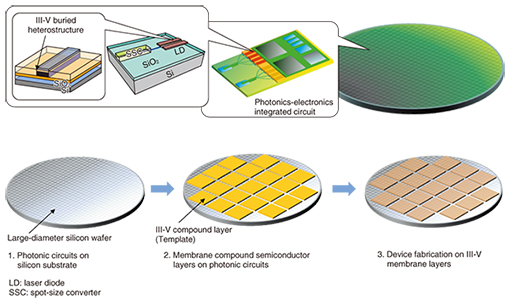
1. IntroductionThe power consumption in information and communication technology devices has reached a critical level with the explosive increase in network traffic. The power dissipation in large-scale datacenters is estimated to exceed 1% of all power consumption. It is therefore essential to cut the power consumption of both networks and devices. Data transmission within datacenters consumes 70% of all network traffic handled by datacenters [1]. Optical interconnection, in which the electrical data transmission is replaced with optical data transmission, has been actively developed to reduce datacenter power consumption. Vertical cavity surface emitting lasers (VCSELs) have already been commercialized as the transmitters for intra-rack and inter-board data transmission. Furthermore, optical links for intra-chip data transmission are also attracting attention because the performance of chip-to-chip and intra-chip data transmission for large-scale integrated circuits is facing the limit. To introduce optical links into short-reach data transmission, it is critical to reduce the power consumption and large-scale integration of optical devices, including transmitters and receivers. Wavelength division multiplexing (WDM) is a promising technology to realize large-capacity and low-cost optical links. However, the VCSELs currently used in optical interconnections are inappropriate for single-mode transmission and the WDM network. It is thus essential to achieve high-density integration of single-mode lasers such as distributed feedback (DFB) lasers in order to introduce the WDM network into short-reach optical interconnections. Efforts to achieve high-density integration include the development of silicon photonics to realize low-cost and high-density optical device integration on large-diameter silicon wafers [2]. The use of silicon photonics is expanding from passive components such as optical waveguides and filters to active components such as modulators and germanium-based photodiodes. In addition, the fusion of optical and electronic circuits is promising. Transceivers consisting of silicon optical devices and CMOS (complementary metal-oxide-semiconductor) transistors integrated on silicon wafers have already been commercialized. Meanwhile, the integration of lasers on silicon remains a challenge. Silicon is an indirect transition semiconductor; it is not appropriate for light sources because of its extremely low emission efficiency. Some approaches have been proposed to achieve emission of silicon-based materials. These approaches include adding impurities, enhancing the emission rate by using fine structures, and using germanium-based lasers. However, commercialized lasers have not been achieved yet. The standard approach is hybrid integration of compound semiconductor-based lasers and silicon-based optical devices. The commercialized transceivers still employ semiconductor lasers as extra light sources. There are two ways of achieving hybrid integration: laser bonding on silicon optical circuits, and laser fabrication on compound semiconductor active regions bonded on silicon waveguides. The former approach requires fine alignment between the lasers and silicon waveguides with submicron order accuracy. This requirement will raise the fabrication cost as the integration density increases. In the latter approach, laser waveguides are determined by the silicon waveguide; therefore, the alignment accuracy of bonding processes is eased. However, it is difficult to achieve compact lasers because the optical confinement in the active layer is low; most optical power is confined in the silicon waveguides. Therefore, it is essential to make progress in both the fabrication process and the development of the laser structure in order to realize high-density integration of lasers with low-power consumption on silicon substrates. 2. Integration of compound semiconductors on a silicon substrateNTT has developed novel techniques to integrate semiconductor lasers on silicon. The concept of the integration is shown in Fig. 1. First, silicon photonic circuits are fabricated on a large-diameter silicon dioxide and silicon (SiO2/Si) substrate. Next, membrane compound semiconductor layers are bonded on the silicon photonic circuits. We call this bonded compound semiconductor layer a template. The lasers are fabricated on this template. The lasers can be fabricated by using alignment marks made on a silicon substrate. It is easy to achieve fine alignment between the silicon waveguides and the lasers. This technique will enable high-density integration of all optical devices on a large-diameter silicon wafer. With further development of the integration of photonic and electronic circuits, it will be possible to achieve compact transceivers on a large-scale silicon wafer.
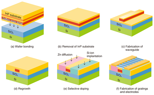
The process used to fabricate the membrane lasers is shown in Fig. 2; it is the same as that described in our previous reports [3–4]. An active layer is grown on an indium phosphide (InP) substrate to be bonded with an SiO2/Si substrate. The InP-substrate is removed to form a membrane layer. The buried heterostructure (BH) is formed by means of waveguide etching and crystal regrowth on the template. The lateral current injection structure is formed by selective impurity doping. Electrodes and Bragg gratings are formed on the surface of the laser. This laser features high optical confinement in the active region thanks to the large difference in the refractive index between SiO2 and the thin compound semiconductor layers. In addition, the BH provides strong carrier confinement in the active region to enhance the carrier-photon interaction. This feature contributes to reducing the footprint and power consumption of lasers [5]. We previously reported the energy cost of 171 fJ/bit, which was the smallest value of all DFB lasers [6]. These approaches enable the high-density integration of silicon optical circuits and high-performance lasers on a silicon wafer.
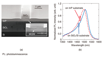
3. Membrane lasers on a silicon substrateWe fabricated the lasers using the fabrication process described in the previous section [7]. The most challenging step is growing the crystal on the bonded wafer consisting of silicon, SiO2, and compound semiconductors. The environmental temperature varies between room temperature and 600°C during the fabrication process. Meanwhile, the thermal expansion coefficients of the silicon, SiO2, and InP are different. This difference causes thermal stress in the epitaxial layer during the fabrication. The stress could cause serious defects in the active region, which would degrade the lasing characteristics. We were able to suppress the effect of thermal stress by using a thin InP-based template. The critical thickness of the InP layer was theoretically estimated to be 430 nm to achieve crystal growth under the temperature variation during the fabrication process. This thickness is sufficient to realize optimized membrane lasers. We used a 250-nm-thick InP-based template to fabricate the lasers. The template is fabricated using a 2-inch-diameter thermally oxidized silicon wafer and an InP wafer. The active layer, consisting of six InGaAsP (indium gallium arsenide phosphide)-based quantum wells, is grown on an InP substrate by metal-organic vapor phase epitaxy (MOVPE). Covalent bonding assisted by O2 plasma is used to bond the epitaxial layer and the SiO2/Si wafer. After the bonding process, the BH is fabricated by chemical etching and MOVPE regrowth. The p-i-n diode structure is formed by Si-ion implantation for n-doped regions and Zn thermal diffusion for p-doped regions. The surface grating is patterned on the 130-nm-thick SiO2 layer above the active region waveguide. A cross section of the fabricated BH is shown in Fig. 3(a). The active region was successfully buried with the InP layer. No cracks or dislocations are observed. The photoluminescence spectrum of the fabricated BH on the SiO2/Si layer is shown in Fig. 3(b). The emission spectrum of BH active layers grown on InP is superimposed. The spectra are almost the same; no serious degradation is observed after the laser fabrication. These results verify that our approach is applicable to laser fabrication.
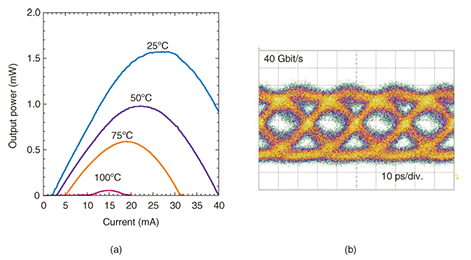
We fabricated the DFB laser by using this active layer. The laser cavity is formed by the surface grating and etching mirrors at the facets. The coupling coefficient of the grating was designed to be 150 cm−1. Single-mode lasing with a side mode suppression ratio over 40 dB is observed. The current-output power characteristics of the fabricated laser with a cavity length of 120 μm are plotted in Fig. 4(a). The threshold current was 1.8 mA. Lasing without kinks is observed at temperatures up to 100°C. An eye diagram of 40-Gbit/s direct modulation is shown in Fig. 4(b). The bias current and modulation voltage were 15 mA and 1.31 V, which corresponds to an energy cost of 848 fJ/bit. The modulation efficiency was 6.0 GHz/mA0.5. This is the first 40-Gbit/s direct modulation of membrane lasers.
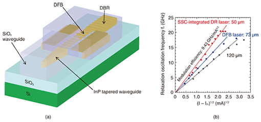
The integration of the lasers and silicon/silica-based waveguide is a significant step forward toward realizing photonic integrated circuits on silicon. A distributed reflector (DR) laser integrated with a spot-size converter (SSC) and a SiOx waveguide [8] is shown in Fig. 5(a). The DR laser consists of a front DFB section and a rear distributed Bragg reflector (DBR) section. The rear DBR mirror suppresses the output from the rear section, which can enhance the effectiveness. A compact cavity can be achieved by employing a DBR with high reflectivity. The BH active region has almost the same structure as that of the previous DFB laser. The surface grating is patterned on the InP surface above the DFB and DBR section. The coupling coefficient is designed to be 1500 cm−1. The SSC section consists of an InP tapered waveguide section covered with the output SiOx waveguide and is formed in front of the DR laser. The laser beam, strongly confined in the BH active region, spreads in the tapered region to convert into the propagation mode of the SiOx waveguide. The DFB length and the SSC taper length are 50 μm and 300 μm, respectively. The measured coupling between the laser and optical fiber is 2.7 dB, which is almost 6 dB smaller than the coupling between the laser without the SSC and a lensed fiber. The modulation efficiency of the fabricated lasers integrated on silicon is plotted in Fig. 5(b). The DFB lasers with cavity lengths of 73 μm and 120 μm, and the DR laser with a cavity length of 50 μm are compared. The modulation efficiency of the DR laser was enhanced to 9.43 GHz/mA0.5 thanks to the short cavity. The energy cost was also improved to 132 fJ/bit under the modulation speed of 25.8 Gbit/s.
4. SummaryWe reported the development of semiconductor lasers fabricated on a silicon substrate. The crystal growth on the bonded wafer makes it possible to achieve membrane lasers operating with low power consumption comparable to VCSELs. We also successfully integrated the laser and the silica-based waveguide with high coupling efficiency. Our next challenges are to achieve high-density integration of the lasers and a larger wafer size. The integration of light sources and silicon optical circuits would greatly expand the application area of silicon photonics. These technologies would pave the way to achieving large-scale optical circuits for optical interconnections. The ultimate target in the future is the integration of electronics and optical circuits. References
|
||||||||||||||||||