|
|||||||||||
|
|
|||||||||||
       |
Feature Articles: Device Technology Development for Beyond 100G Optical Transport Network Vol. 14, No. 9, pp. 1–5, Sept. 2016. https://doi.org/10.53829/ntr201609fa1 Device Technology Development for Beyond 100G Optical Transport NetworkAbstractThe capacity of the optical transport network has been expanding for over 30 years, which has enriched the communication environment of users. This expansion has also helped to reduce the cost of communication lines and facilitate the growth of the Internet and the widespread use of smartphones. In the near future, an optical transport network with a capacity beyond 100 Gbit/s per wavelength (beyond 100G optical transport network) and its device technology will be needed in order to provide more sophisticated communication services such as IoT (Internet of Things) and 5G (fifth-generation) mobile access. This article reviews NTT laboratories’ development of device technology for the beyond 100G optical transport network. Keywords: optical transport network, device technologies, beyond 100G
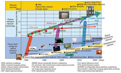
1. IntroductionExpectations for communication networks have been increasing more and more in recent years. The development of the Internet of Things (IoT) is one example of such an expectation. The IoT is expected to make people’s lives richer by connecting and controlling all things via networks. The fifth-generation (5G) mobile access network, which smoothly bridges numerous users/things and core networks in the IoT world, is also attracting attention. It is an optical transport network whose device technology supports the realization of IoT from the viewpoint of long-haul data transmission. The capacity of the optical network has been expanding for over 30 years, which has enriched people’s communication environment (Fig. 1). From the 1980s to the early 1990s, time-division multiplexing (TDM) techniques were developed to reduce the cost of communication lines and to realize integrated services digital networks (ISDNs). With TDM techniques, the capacity of the optical transport network reached 10 Gbit/s per optical fiber. From the late 1990s through the 2000s, progress was made in wavelength-division multiplexing (WDM) techniques in order to cope with the rapid growth in Internet traffic. WDM techniques finally reached a capacity of 1 Tbit/s per fiber. Digital coherent technology has been applied since the 2010s, which has boosted the capacity to manage drastic increases in traffic caused by the widespread use of smartphones. At present, 8 Tbit/s per fiber capacity has already been realized and utilized in real systems.
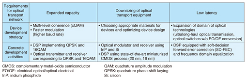
Digital coherent technology is very different from conventional TDM and WDM techniques in terms of the light modulation scheme for carrying digital data. While conventional TDM and WDM techniques use only optical intensity for light modulation, digital coherent technologies modulate not only optical intensity but also the optical phase. Moreover, digital coherent devices can multiplex light polarization, whereas TDM and WDM devices cannot. Because light parameters for carrying digital data are increased in digital coherent technology, the capacity per one wavelength of light has reached 100 Gbit/s at present. (When WDM techniques were the prevailing technology, a few dozen wavelength signals were multiplexed in one optical fiber. At the end of the WDM era, 40-Gbit/s capacity per wavelength had been achieved due to steady progress in TDM techniques.) As mentioned so far, digital coherent technology adopts a more complex light modulation and multiplexing scheme than those of conventional TDM and WDM techniques, and it is the optoelectronic devices that physically realize the complex digital coherent technology. Communication traffic in the world of IoT with 5G mobile access is expected to continue to increase, so an optical transport network beyond 100 Gbit/s per wavelength (hereafter, 100 Gbit/s/λ; λ (lambda) = wavelength), referred to as a beyond 100G optical transport network is highly desirable by people all over the world. 2. Requirements for beyond 100G optical transport network and development strategy for associated devicesThree requirements for the beyond 100G optical transport network and the strategy of developing the optoelectronic devices used with it are summarized in Table 1. NTT laboratories established the development strategy in order to meet the requirements, and development of the optoelectronic devices is underway to achieve the beyond 100G optical transport network. The details of the development strategy are described below.
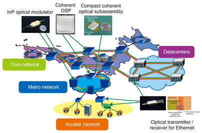
2.1 Expanded capacityCommunication traffic will continue to increase in the next generation, and it will be vital to expand the capacity in order to meet the increase. In particular, it is important to find a way to transport mobile traffic long distances at reasonable cost as soon as possible. Mobile traffic is currently growing at 1.4 times the current amount per year. Although 8-Tbit/s total capacity optical transport systems with 100 Gbit/s/λ were installed in 2013, 30-Tbit/s-class systems with 400 Gbit/s/λ are expected to be necessary by 2017 to support the growing mobile traffic. Optoelectronic devices used for such optical transport systems should be ready one year ahead of the time they are needed; therefore, research and development (R&D) of optoelectronic devices must be done quickly and efficiently. NTT laboratories have been focusing on digital coherent technology as a way to expand the capacity of the optical transport network. R&D is underway on more sophisticated modulation schemes such as 16-level quadrature amplitude modulation (16QAM), as well as conventional optical modulation schemes such as quadrature phase-shift keying (QPSK). We are also working to increase the speed of modulation (baud rate). By combining a more sophisticated modulation scheme and a faster baud rate, we will be able to achieve a much larger capacity of the optical transport network in the near future. One concrete example of this is that NTT laboratories are trying to implement a more sophisticated modulation scheme and a faster baud rate into a digital signal processor (DSP), which is the heart of the optical transport network utilizing digital coherent technology. As for the optical transmitter and receiver, we are focusing especially on the coexistence of highly linear input-output characteristics and faster performance, which are essential for implementing a more sophisticated modulation scheme and faster baud rate. 2.2 Downsizing of optical transport equipmentThe volume of optical transport equipment affects the size of the facility of the communication carrier company, so compact assembly/packaging is essential. If the communication traffic is increased several times with the new equipment, the volume of the equipment will need to be equal in size or smaller than the previous equipment. In recent years, not only have the facilities of communication carrier companies been directly connected to the optical transport network in order to deliver information long distances, but so too have datacenters run by information technology companies. The allotted space for equipment in datacenters is very limited, so compact assembly/packaging is mandatory when installing optoelectronic devices in datacenters. Two aspects in the R&D of optoelectronic devices that are important in order to achieve compact assembly/packaging are: 1) making each device smaller, and 2) reducing power consumption to prevent the inevitable problem of heat radiation in smaller size devices. For example, although a 100-Gbit/s/λ digital coherent optical transceiver (commercialized in 2013) has a footprint of 5 inches × 7 inches (12.70 cm × 17.78 cm), a 1.6 inch × 4.2 inch CFP2-ACO (centum (100) gigabit form-factor pluggable 2 - analogue coherent optics, 4.06 cm × 10.67 cm) optical transceiver has been developed and is being commercialized in 2016. From now on, making devices smaller and reducing power consumption will remain important tasks, and progress in these areas will continue rapidly. To make devices smaller, NTT laboratories choose appropriate materials for optoelectronic devices and optimize the device design. Selecting high refractive index materials such as indium phosphide (InP) and silicon (Si) helps in reducing the sizes of optoelectronic devices, but we are also focusing on optimizing the device design so as not to degrade the optical transport performance. Also, to reduce power consumption, NTT laboratories have been researching and developing ways to reduce the driving voltage of optical modulators. Optical modulators using InP are a representative example of such development, and the details are described in the other Feature Articles in this issue. As for DSP, the use of a state-of-the-art complementary metal-oxide semiconductor (CMOS) miniaturized process made it possible to achieve a drastic reduction in power consumption. While 40-nm and 20-nm CMOS miniaturized processes were used in developing the DSP, a 16-nm process—the first in the world—is being used in the most recent development to further reduce power consumption. 2.3 Low latencyIn the near future, many applications using the communication network will be introduced. These applications include those for services that require real-time responses and that have low latency. Examples for such services include highly sophisticated financial services and smart cars connected to the communication network. The total latency of network services mainly depends on the configuration of servers and the architecture of the network. However, in terms of the optical physical layer, reducing the latency inside the optical transport equipment is effective in reducing the overall latency. The most effective way to reduce latency is to reduce the number of times data packets are stored and forward-processed after optical-to-electrical (OE) conversion, or in other words, to reduce the number of core routers. Moreover, if OE and electrical-to-optical (EO) conversions were excluded as well as the decreased number of core routers, much lower latency would be obtained. These technical trends require expanding the domain of optical technologies, for example, extending the transmission distance of optical signals without OE/EO conversion relay and routing optical signals without the OE/EO process. To contribute to the low latency of the communication network using optical technologies, NTT laboratories have been researching ways to extend the reach of optical signals in the optical transport network and investigating switching techniques that do not require OE/EO conversions. The following Feature Articles introduce NTT’s development of a DSP implementing soft-decision forward error correction (SD-FEC) and frequency domain equalization to extend the optical transmission distance. 3. Future overviewThe final goal of NTT laboratories, especially NTT Network Innovation Laboratories and NTT Device Innovation Center, is the widespread use of the beyond 100G optical transport network. To achieve this goal, we are continuing our R&D on state-of-the-art technologies and fabrication of easy-to-use devices in a timely manner based on the development strategy described earlier. The Feature Articles in this issue introduce the following devices, which have been developed according to this strategy (Fig. 2).
(1) Coherent DSPs: These are the heart of the optical transport network with digital coherent technology [1] (2) InP coherent optical modulators and compact coherent optical subassembly: These have the compact size needed for the next generation of optical transport equipment and achieve adequate performance by working in conjunction with coherent DSPs [2, 3] (3) Optical transmitter and receiver for high-speed optical Ethernet: These are essential optical components for connection between routers/switches in client-side and coherent systems [4] References
|
||||||||||