|
|||||||||||||||||||||||
|
|
|||||||||||||||||||||||
       |
Feature Articles: State-of-the-art Space Division Multiplexing Technologies for Future High-capacity Optical Transport Networks Vol. 15, No. 6, pp. 16–22, June 2017. https://doi.org/10.53829/ntr201706fa3 Dense Space Division Multiplexing (DSDM) Photonic-node Platform TechnologyAbstractOptical infrastructure networks transporting high-volume traffic have been built using photonic node technologies such as optical signal transmission, optical signal wavelength multiplexing and demultiplexing, and reconfigurable optical add/drop multiplexers. This article gives an overview of photonic nodes using dense space division multiplexing technology and their potential for implementing high-capacity optical networks. Keywords: space division multiplexing, optical node architectures, integrated wavelength selective switching technology
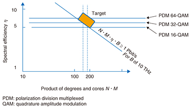
1. IntroductionCommunication traffic continues to increase each year, and the total Internet traffic in Japan alone reached 5.4 Tbit/s in 2015, increasing by 50% in that year [1]. If we assume a 40% increase per year, we can predict that the volume will exceed 1 Pbit/s by the mid-2020s. The capacity of single-mode fiber (SMF) is estimated to be 100 Tbit/s. To overcome the capacity limitations of SMF, research is underway on transport technologies using dense space division multiplexing (DSDM) [2]. It is also expected that DSDM will similarly need to be used to handle high-volume traffic in the photonic nodes used to build optical transport networks [3]. The throughput of a photonic node S is given by the product of the number of degrees N, the number of cores M, the spectral efficiency η, and the desired bandwidth B. The relationships between the number of degrees, number of cores, spectral efficiency, and attainable throughput are shown in Fig. 1. The two main bands used for optical communication are the 1.55-μm band (C band) and the 1.58-μm band (L band), which together give a combined 10 THz of usable bandwidth. The solid line in the figure shows the relationship between spectral efficiency and the space division multiplicity (product of degrees and cores N•M), to implement an optical node with a throughput of 1 Pbit/s, assuming a combined signal bandwidth of 10 THz for the C band and L band. Achieving 10-Pbit/s-class throughput using modulation with the multiplicity of polarization-division-multiplexed 16-quadrature amplitude modulation (PDM 16-QAM) or greater, which would give a spectral efficiency of 5 bit/s/Hz or better, would give η of 5 to 6 bit/s/Hz. Therefore, with the desired bandwidth B = 10 THz, space division multiplexing (SDM) photonic nodes with the product of cores and degrees N•M of 150 to 200 would be needed. Thus, with eight degrees, photonic nodes using DSDM with more than 20 cores would be necessary. Wavelength selective switches (WSS) already used to build reconfigurable optical add/drop multiplexers (ROADM) have around 20 ports, but there are issues in using them for high-capacity DSDM photonic nodes.
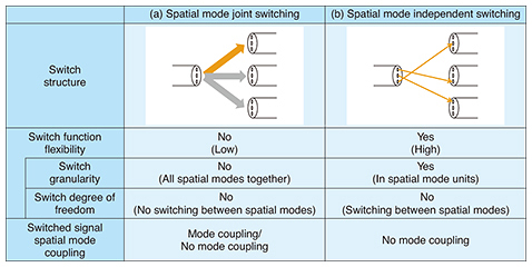
This article gives an overview of the devices and methods necessary to implement photonic nodes with DSDM technology for high-capacity optical networks. 2. DSDM photonic node structure and SDM photonic networksDSDM photonic nodes introduce a new degree of freedom in the spatial domain and with it, additional complexity to the node structure. For this reason, it is a challenge to implement a simple DSDM photonic node that provides the switching function necessary for an SDM photonic network. 2.1 Spatial mode switching typesDSDM photonic nodes can be broadly categorized into (a) spatial mode joint switching and (b) spatial mode independent switching, according to whether they can switch spatial modes independently or not (Table 1). SDM transmission methods include multi-core fiber (MCF), which involves multiple cores within a single optical fiber, and multi-mode fiber (MMF), which involves multiple waveguide modes propagating within a single core. We use spatial modes to refer to cores within MCF and waveguide modes within MMF. Spatial mode joint switching switches all spatial modes in a single optical fiber at once, outputting them to the same optical fiber. In contrast, spatial mode independent switching can independently select the output optical fiber for each spatial mode.
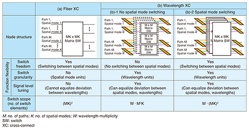
When MMF is used, the spatial modes (waveguide modes) of the optical signal are coupled, so multiple modes are transmitted and received together, and the receiver must process the signal to separate these modes. All waveguide modes input to a single optical fiber are output from the fiber, so spatial mode joint switching is adequate. However, if MCF is used, coupling between spatial modes (cores) is weak, so optical signals from different transceiver nodes can be transmitted on each spatial mode. The use of spatial mode independent switching rather than joint switching for this yields finer switching granularity and more flexible switching control. 2.2 Switching methods according to switching granularity and degree of freedomDSDM photonic node structures for spatial mode independent switching are listed in Table 2. They are classified according to whether they can switch wavelengths independently (wavelength independence) and whether they can switch between spatial modes. With SDM transmission, multiple optical signals with different wavelengths can be multiplexed and transmitted in each core or in each waveguide mode. DSDM photonic node structures can be classified as either (a) fiber cross-connect (fiber XC), which switches all wavelengths of the optical signal in a single spatial mode at once, or (b) wavelength cross connect (wavelength XC), which can switch wavelengths independently. Table 2 also lists wavelength XCs further classified into those that can or cannot switch signals between spatial modes. In these structures, the switching granularity gets finer moving from fiber XC to wavelength XC, and the degree of freedom in switching increases by enabling switching between spatial modes, providing greater flexibility in switching control.
Table 2 also indicates the signal level tuning and the scale (number) of switches needed to implement each node structure. The wavelength XC configuration with spatial mode switching ((b)-2) has very flexible switching control and is able to adjust levels to reduce disparity among both optical signal spatial modes and wavelengths in transmission paths and nodes. However, it requires more switch elements, so a simple node implementation is difficult to achieve. Network control technologies such as software-defined networking (SDN)*1 are expected to advance in the future, and in line with this, network control techniques providing greater flexibility will be needed. Research is underway at the NTT laboratories on wavelength XC as a DSDM photonic node structure that will enable more-flexible switching control, as it can switch independently between spatial modes. To allocate network resources efficiently in a network using DSDM photonic nodes, the degree of freedom in the spatial domain must be considered. As SDM photonic networks are expanded, network capacity will need to be designed so as to optimize resource utilization. Wavelength domain resources on communication routes will have to be allocated in the network using conventional wavelength division multiplexing (WDM), but spatial domain resources will also have to be allocated. The transmission characteristics of the optical fiber medium (MCF or MMF) and photonic nodes are also conditions of signal capacity. Thus, optical fiber characteristics and photonic node structures are very important elements in SDM photonic networks.
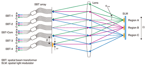
3. DSDM photonic node switching devicesMultiple switching devices are used in a DSDM photonic node. SDM technology is expected to be used together with WDM communication to increase throughput, so a WSS able to switch by wavelength is needed. Thus, a structure with multiple WSS is needed in an SDM photonic network, and the increased footprint of node equipment could become a concern. We are developing a spatial and planar optical circuit (SPOC) platform [4] combining waveguide optical systems*2 and spatial optical systems*3, which is an original optical system technology integrating multiple WSS in a single module. A schematic diagram of an optical system integrating multiple WSS using the SPOC platform is shown in Fig. 2. The spatial beam transformer (SBT) circuit elements, positioned on optical waveguides, play an important role in integrating the multiple WSS. The SBT circuits are composed of a slab waveguide and an array waveguide with uniform lengths. When the light signal shown with pink arrows is input to the SBT circuit designated as SBT-Com in Fig. 2, it diverges in the plane of the slab waveguide and is output to the spatial optical system through the array waveguides. Here, the lengths of the array waveguides are the same, so the wavefront of the output optical signal is planar, with the direction shown by the pink dotted line. When the light signal is switched to the green input port, the output optical signal will be a planar wave in the direction of the green upwardly inclined dotted line. The optical signals arrive at a different position on the spatial light modulator (SLM), which is the switching engine, and are independently reflected in different directions. Finally, the signals are independently switched to any of the output ports and optically combined at the output SBT circuits.
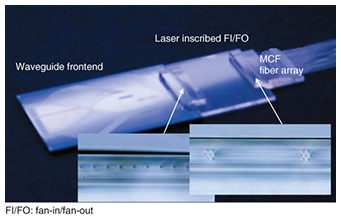
We constructed a WSS for MCF [5] using this multiple-WSS integrated function. A photograph of the optical waveguide system on the SPOC platform is shown in Fig. 3. The MCF has a two-dimensional (2D) core arrangement, so to combine it with the planar optical waveguide, the two dimensions must be converted to one dimension. In this case, we fabricated a circuit to convert the core arrangement from 2D to 1D using 3D waveguide technology with an ultrashort pulse laser*4 and implemented a direct connection of the MCF to the waveguide circuits.
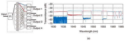
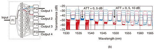
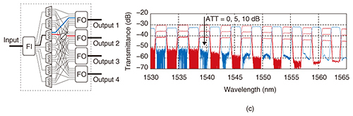
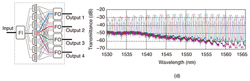
The switching spectra for each core of a 1 x 4 WSS for a 7-core MCF are shown in Fig. 4. Here, operation is configured as a flexible grid with different wavelength bands for wavelength channels on the first and seventh cores (see Fig. 4(a)), as two-way switching and attenuation with a 200-GHz channel width on the second (Fig. 4(b)) and third cores (Fig. 4(c)), and as switching to four different paths with a 50-GHz channel width on cores 4 to 6 (Fig. 4(d)).
Each of these examples implements wavelength selective switching operation, showing that the SPOC platform is effective for SDM node switches.
4. Future prospectsThe SPOC platform is a key technology for making DSDM photonic nodes smaller. The NTT laboratories will receive support for contracted research from NICT (the National Institute of Information and Communications Technology) and other institutions and conduct research and development (R&D) through open innovation [6] to accelerate R&D on these elemental technologies. References
|
||||||||||||||||||||||