
You need Adobe Reader 7.0 or later in order to read PDF files on this site.
If Adobe Reader is not installed on your computer, click the button below and go to the download site.

|
Regular Articles
Vol. 16, No. 5, pp. 27–32, May 2018. https://doi.org/10.53829/ntr201805ra1
Digital-preprocessed Analog-multiplexed Digital-to-analog Converter for Ultrahigh-speed Optical Transmitter
Hiroshi Yamazaki,
Munehiko Nagatani,
Fukutaro Hamaoka,
Masanori Nakamura,
Toshikazu Hashimoto,
Hideyuki Nosaka,
and Yutaka Miyamoto
Abstract
We have developed technology to extend the analog bandwidth of digital-to-analog converters (DACs), which are essential in advanced high-speed optical transmitters. We used a digital preprocessor, two sub-DACs, and an analog multiplexer to generate arbitrary signals with a bandwidth nearly twice that of each sub-DAC. This technology was used to successfully demonstrate various high-speed transmissions, including an intensity-modulated directly detected transmission at a record-high data rate of 250 Gbit/s.
Keywords: DSP, DAC, analog multiplexer
1. Introduction
The continued growth of data traffic in communications systems has resulted in the need to find ways to increase data rates of optical transmission systems [1]. Digital signal processors (DSPs) play key roles in current high-speed transmission systems [2, 3]. Functions of the DSPs include high-order modulation, pulse shaping, equalization, and dispersion compensation, which are essential for achieving high data rates with high spectral efficiency.
In a DSP-based transmitter, the analog bandwidth of digital-to-analog converters (DACs) is a key factor to determine the achievable data rate. The DACs used in commercial transmitters today are fabricated on silicon complementary metal-oxide semiconductor (CMOS) platforms and integrated with DSPs monolithically [2, 3]. Those CMOS DACs have a rather moderate analog bandwidth of ~30 GHz, which is one of the factors limiting the data rate.
DACs based on compound platforms such as indium phosphide (InP) or SiGe (silicon-germanium) provide larger bandwidth [4–6], but they consume more power. Compound DACs also pose some implementation challenges because the DSP will continue to be based on CMOS technology. This is why there is a strong need to develop technologies to extend the bandwidth using existing CMOS DACs.
We have developed a digital-preprocessed analog-multiplexed DAC (DP-AM-DAC) that is a promising potential solution in this context [7–10]. The DP-AM-DAC consists of a digital preprocessor, two sub-DACs, and an analog multiplexer (AMUX) and functions as a DAC with an analog bandwidth of almost twice that of each sub-DAC. We have generated signals with bandwidths of up to ~60 GHz with CMOS sub-DACs and an AMUX based on an InP heterojunction bipolar transistor (HBT). Unlike other bandwidth-extension technologies that use analog mixers [3, 11], the DP-AM-DAC has a symmetric configuration with respect to the two sub-DACs and so makes it easier to balance the two branches. In this article, we review our DP-AM-DAC and the high-speed transmission experiments conducted with it.
2. Principle
The configuration and principle of the DP-AM-DAC is shown in Fig. 1. It consists of a digital preprocessor, two sub-DACs, and an AMUX [7–10]. When the bandwidth of the sub-DACs is fB/2, we can obtain an arbitrary signal with a bandwidth up to around fB (twice that of the sub-DACs) as the final output from the AMUX. The schematic spectra in Fig. 1 represent the principle of the DP-AM-DAC, in which the AMUX is driven at fclk = fB [7].
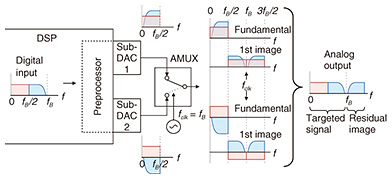
Fig. 1. Configuration and principle of DP-AM-DAC (type I).
First, the digital representation of the target signal with a bandwidth up to fB is input to the preprocessor. The preprocessor weaves the information of the target signal into two digital sub-signals with a corresponding bandwidth of fB/2 or less so that the sub-DACs can handle them without loss of information. Specifically, the preprocessor separates the input signal into low- and high-frequency components—respectively represented by red and blue—and then flips the high-frequency component around fB/2 in the frequency domain. Finally, the processor adds the flipped high-frequency component to the low-frequency component with a specific amplitude ratio and complementary phases to make the two respective sub-signals.
The sub-DACs convert the digital sub-signals into the analog sub-signals, which pass alternately through the AMUX at a clock frequency of fclk. In the frequency domain, this alternation, or multiplexing, corresponds to a superposition of the sub-signals themselves and their images (up-converted copies) generated around fclk, where the phases of the images for the two sub-signals are complementary to each other. As seen in Fig. 1, the superposition results in the reconstruction of the target signal in the frequency region of 0 < f < fB. The residual image of the high-frequency component in the frequency region of fB < f < 3fB/2 can be removed by a low-pass filter. The principle explained above is what we call the type-I DP-AM-DAC. We have also developed the type-II model, which has the same hardware configuration as the type-I model but uses a different preprocessing algorithm so that we can reduce the required fclk by half and suppress the residual image [8].
3. AMUX characteristics
The key component in the DP-AM-DAC is the AMUX, which we designed and fabricated using our in-house 0.5-μm-emitter InP HBT technology [12]. As mentioned above, the AMUX is a linear high-speed selector that makes two input signals pass through it alternately at the clock frequency without any regeneration. Time-domain waveforms we measured to verify the AMUX are shown in Fig. 2. We input a 1-GHz sinusoidal wave to one input port while applying direct current (DC) voltage to the other and varied the clock frequency. The obtained output waveforms show that the AMUX selects the two inputs alternately at the clock frequency, as designed.
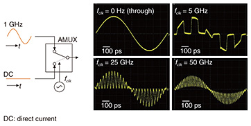
Fig. 2. Time-domain waveforms output from the AMUX multiplexing a 1-GHz sinusoidal wave and DC voltage at clock frequencies of 0, 5, 25, and 50 GHz.
The static frequency responses of the AMUX module are shown in Fig. 3. The response is measured by applying DC voltage to the clock port to select and deselect the input analog signal under test to measure the through and isolation characteristics, respectively. Up to the measured frequency range of 50 GHz, the through loss is less than 3 dB, while the isolation (the difference between the two curves) is more than 20 dB.
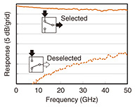
Fig. 3. Static frequency responses of AMUX when the input signal is selected and deselected.
4. Transmission results
The DP-AM-DAC was first demonstrated in a high-speed intensity-modulated direct-detection (IMDD) transmission, in which we employed Nyquist-shaped 80-Gbaud (160-Gbit/s) four-level pulsed amplitude modulation (PAM4) [7]. The experimental setup is shown in Fig. 4. We used two channels of a CMOS-based arbitrary waveform generator (AWG) as the sub-DACs with an analog 3-dB bandwidth of ~20 GHz. The signal was generated using the type-I DP-AM-DAC at fclk = 43.3 GHz. As the optical transmitter, we used an O-band (1.3-μm) externally modulated laser with a modulation bandwidth of > 55 GHz [13]. The optical signal was transmitted over 20-km standard single-mode fiber (SSMF) and then amplified by a fiber amplifier and received by a photodiode. The DSP, including the preprocessor of the DP-AM-DAC, the receiver-side filter, and an adaptive equalizer (AEQ) was emulated by an offline personal computer.
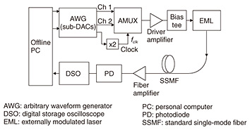
Fig. 4. Experimental setup for high-speed IMDD transmission experiments using the DP-AM-DAC.
The electrical spectra of the output signals from the two sub-DACs and the AMUX are shown in Fig. 5(a)–(c). Although the signals from the sub-DACs have a bandwidth of only ~22 GHz, that from the AMUX includes a rectangular waveform with a bandwidth of ~40 GHz, which corresponds to the target 80-Gbaud Nyquist PAM4 signal. The residual image at > 46 GHz observed in the AMUX output was removed by the receiver-side matched filter in this experiment.
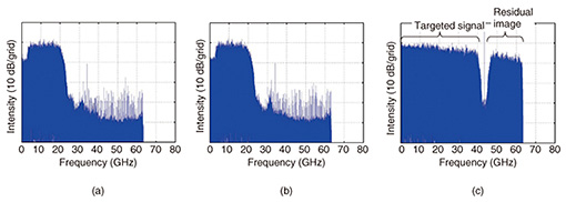
Fig. 5. Electronic spectra of output signals from (a) sub-DAC channel 1, (b) sub-DAC channel 2, and (c) AMUX measured in the 80-Gbaud PAM4 transmission experiment.
The eye diagram of the 80-Gbaud (160-Gbit/s) PAM4 signal after transmission over 20-km SSMF and through the digital matched filter and the AEQ is shown in Fig. 6. The bit error rate (BER) was 6.2 x 10⁻³. This result corresponds to the net data rate of 142.9 Gbit/s, assuming the use of 12%-overhead (OH) hard-decision forward error correction (FEC) code [14].
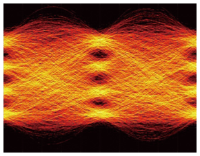
Fig. 6. Eye diagram of 80-Gbaud PAM4 signal after 20-km SSMF transmission and digital AEQ.
We also demonstrated a higher net data rate of 250 Gbit/s with the type-II DP-AM-DAC [8]. The setup was similar to the one shown in Fig. 4, but the sub-DACs (AWG) were upgraded to those with an analog 3-dB bandwidth of ~32 GHz, and the fclk was changed to 37.5 GHz. With the type-II principle, we can generate signals with the analog bandwidth up to 2fclk = 75 GHz, although the bandwidth used in the experiment was limited to 62 GHz by the bandwidth of the DSO (digital storage oscilloscope). We employed discrete multitone (DMT) modulation [15] to efficiently utilize the available bandwidth. The electronic spectrum and constellations of the received DMT signal at the total bit rate of 300.12 Gbit/s after transmission over 10-km SSMF are shown in Fig. 7. The total BER was 2.63 x 10⁻², which is lower than the threshold of the 20%-OH soft-decision FEC code [16], and it corresponds to the transmission at a net data rate of 250 Gbit/s.
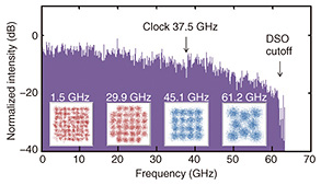
Fig. 7. Electronic spectrum and constellations of the 300.12-Gbit/s DMT signal after 10-km SSMF transmission.
In addition to the results described above, we have reported various high-speed transmission experiments utilizing DP-AM-DACs, including long-haul digital coherent transmission [17–20].
5. Conclusion
With the DP-AM-DAC, we can overcome the bandwidth limitation imposed by the analog bandwidths of CMOS DACs. The combination of the digital preprocessor, two CMOS sub-DACs, and the high-speed AMUX enables us to generate arbitrary signals with a bandwidth nearly twice that of each sub-DAC. This technology is promising for use in future ultrahigh-speed optical transmitters for various application fields, including short-reach IMDD and long-haul digital coherent systems.
References
| [1] | Y. Miyamoto, “Over 400 Gbit/s Digital Coherent Channels for Optical Transport Network,” Proc. of the 21st OptoElectronics and Communications Conference/International Conference on Photonics in Switching 2016 (OECC/PS 2016), ThB3-1, Niigata, Japan, July 2016. |
|---|
| [2] | O. Ishida, K. Takei, and E. Yamazaki, “Power Efficient DSP Implementation for 100 G-and-beyond Multi-haul Coherent Fiber-optic Communications,” Proc. of the 39th Optical Fiber Communication Conference and Exhibition (OFC 2016), W3G.3, Anaheim, CA, USA, Mar. 2016. |
|---|
| [3] | C. Laperle and M. O’Sullivan, “Advances in High-speed DACs, ADCs, and DSP for Optical Coherent Transceivers,” J. Lightw. Technol., Vol. 32, No. 4, pp. 629–643, 2014. |
|---|
| [4] | M. Nagatani, H. Wakita, H. Nosaka, K. Kurishima, M. Ida, A. Sano, and Y. Miyamoto, “75 GBd InP-HBT MUX-DAC Module for High-symbol-rate Optical Transmission,” Electron. Lett., Vol. 51, No. 9, pp. 710–712, 2015. |
|---|
| [5] | A. Konczykowska, F. Jorge, J.-Y. Dupuy, M. Riet, V. Nodjiadjim, H. Aubry, and A. Adamiecki, “84 GBd (168 Gbit/s) PAM-4 3.7 Vpp Power DAC in InP DHBT for Short Reach and Long Haul Optical Networks,” Electron. Lett., Vol. 51, No. 20, pp. 1591–1593, 2015. |
|---|
| [6] | K. Schuh, F. Buchali, W. Idler, Q. Hu, W. Templ, A. Bielik, L. Altenhain, H. Langenhagen, J. Rupeter, U. Dümler, T. Ellermeyer, R. Schmid, and M. Möller, “100 GSa/s BiCMOS DAC Supporting 400 Gb/s Dual Channel Transmission,” Proc. of the 42nd European Conference on Optical Communication (ECOC 2016), M.1.C.4., Dusseldorf, Germany, Sept. 2016. |
|---|
| [7] | H. Yamazaki, M. Nagatani, S. Kanazawa, H. Nosaka, T. Hashimoto, A. Sano, and Y. Miyamoto, “Digital-preprocessed Analog-multiplexed DAC for Ultra-wide-band Multilevel Transmitter,” J. Lightw. Technol., Vol. 34, No. 7, pp. 1579–1584, 2016. |
|---|
| [8] | H. Yamazaki, M. Nagatani, F. Hamaoka, S. Kanazawa, H. Nosaka, T. Hashimoto, and Y. Miyamoto, “Discrete Multitone Transmission at Net Data Rate of 250 Gb/s Using Digital-preprocessed Analog-multiplexed DAC with Halved Clock Frequency and Suppressed Image,” J. Lightw. Technol., Vol. 35, No. 7, pp. 1300–1306, 2017. |
|---|
| [9] | H. Yamazaki, M. Nagatani, S. Kanazawa, H. Nosaka, T. Hashimoto, F. Hamaoka, and Y. Miyamoto, “Discrete Multi-tone Transmitter at Net Data Rate of 200 Gbps Using a Digital-preprocessed Analog-multiplexed DAC,” Proc. of ECOC 2016, Tu.3.C.2, Dusseldorf, Germany, Sept. 2016. |
|---|
| [10] | H. Yamazaki, M. Nagatani, F. Hamaoka, K. Horikoshi, M. Nakamura, A. Matsushita, S. Kanazawa, T. Hashimoto, H. Nosaka, and Y. Miyamoto, “Ultra-high-speed Optical Transmission Using Digital-preprocessed Analog-multiplexed DAC,” Opt. Commun., Vol. 409, No. 15, pp. 66–71, 2018. |
|---|
| [11] | X. Chen, S. Chandrasekhar, S. Randel, G. Raybon, A. Adamiecki, P. Pupalaikis, and P. Winzer, “All-electronic 100-GHz Bandwidth Digital-to-analog Converter Generating PAM Signals up to 190-GBaud,” J. Lightw. Technol., Vo. 35, No. 3, pp. 411–417, 2017. |
|---|
| [12] | M. Nagatani, H. Yamazaki, H. Wakita, H. Nosaka, K. Kurishima, M. Ida, A. Sano, and Y. Miyamoto, “A 50-GHz-bandwidth InP-HBT Analog-MUX Module for High-symbol-rate Optical Communications Systems,” Proc. of 2016 IEEE MTT-S International Microwave Symposium (IMS), TU1C-3, San Francisco, CA, USA, May 2016. |
|---|
| [13] | S. Kanazawa, H. Yamazaki, Y. Nakanishi, Y. Ueda, W. Kobayashi, Y. Muramoto, H. Ishii, and H. Sanjoh, “214-Gb/s 4-PAM Operation of Flip-chip Interconnection EADFB Laser Module,” J. Lightw. Technol., Vol. 35, No. 3, pp. 418–422, 2017. |
|---|
| [14] | M. Scholten, T. Coe, J. Dillard, and F. Chang, “Enhanced FEC for 40G/100G,” Proc. of the 35th European Conference on Optical Communication (ECOC 2009), WS1, Vienna, Austria, Sept. 2009. |
|---|
| [15] | W. Yan, T. Tanaka, B. Liu, M. Nishihara, L. Li, T. Takahara, Z. Tao, J. Rasmussen, and T. Drenski, “100 Gb/s Optical IM-DD Transmission with 10G-class Devices Enabled by 65GSamples/s CMOS DAC Core,” Proc. of the 36th Optical Fiber Communication Conference and Exhibition (OFC 2013), OM3H.1, Anaheim, CA, USA, Mar. 2013. |
|---|
| [16] | D. Chang, F. Yu, Z. Xiao, N. Stojanovic, F. N. Hauske, Y. Cai, C. Xie, L. Li, X. Xu, and Q. Xiong, “LDPC Convolutional Codes Using Layered Decoding Algorithm for High Speed Coherent Optical Transmission,” Proc. of the 35th Optical Fiber Communication Conference and Exhibition (OFC 2012), OW1H.4, Los Angeles, CA, USA, Mar. 2012. |
|---|
| [17] | K. Horikoshi, F. Hamaoka, A. Matsushita, M. Nagatani, H. Yamazaki, A. Sano, T. Hashimoto, H. Nosaka, K. Yonenaga, A. Hirano, and Y. Miyamoto, “96Gbaud Nyquist-PDM-QPSK Signal Transmission over 12,120 km Using DP-AM-DAC and Decision-feedback Equalizer,” Proc. of OECC/PS 2016, ThD2-3, Niigata, Japan, July 2016. |
|---|
| [18] | A. Matsushita, F. Hamaoka, M. Nakamura, K. Horikoshi, H. Yamazaki, M. Nagatani, A. Sano, A. Hirano, and Y. Miyamoto, “Super-Nyquist 9-WDM 126 GBaud PDM-QPSK Transmission over 7878 km Using Digital-preprocessed Analog-multiplexed DAC for Long-haul Applications,” Proc. of ECOC 2016, W.3.D.2, Dusseldorf, Germany, Sept. 2016. |
|---|
| [19] | M. Nakamura, F. Hamaoka, A. Matsushita, H. Yamazaki, M. Nagatani, A. Sano, A. Hirano, and Y. Miyamoto, “120 GBaud Coded 8 Dimensional 16QAM WDM Transmission Using Low-complexity Iterative Decoding Based on Bit-wise Log Likelihood Ratio,” Proc. of the 40th Optical Fiber Communication Conference and Exhibition (OFC 2017), W4A.3, Los Angeles, CA, USA, Mar. 2017. |
|---|
| [20] | F. Hamaoka, S. Okamoto, M. Nakamura, A. Matsushita, T. Kobayashi, H. Yamazaki, M. Nagatani, Y. Kisaka, A. Hirano, and Y. Miyamoto, “Experimental Demonstration of Simplified Adaptive Equalizer for Fractionally Sampled 120-GBaud Signal,” Proc. of the 43rd European Conference on Optical Communication (ECOC 2017), P1.SC3.34, Gothenburg, Sweden, Sept. 2017. |
|---|
 |
- Hiroshi Yamazaki
- Distinguished Researcher, NTT Device Technology Laboratories and NTT Network Innovation Laboratories.
He received a B.S. in integrated human studies in 2003 and an M.S. in human and environmental studies in 2005, both from Kyoto University, and a Dr.Eng. in electronics and applied physics from Tokyo Institute of Technology in 2015. He joined NTT Photonics Laboratories in 2005, where he has been researching optical waveguide devices for communication systems. He is concurrently with NTT Network Innovation Laboratories and NTT Device Technology Laboratories, where he is involved in research on devices and systems for optical transmission using advanced multilevel modulation formats. Dr. Yamazaki is a member of the Institute of Electronics, Information and Communication Engineers (IEICE).
|
|---|
 |
- Munehiko Nagatani
- Distinguished Researcher, NTT Device Technology Laboratories and NTT Network Innovation Laboratories.
He received an M.S. in electrical and electronics engineering from Sophia University, Tokyo, in 2007. He joined NTT Photonics Laboratories in 2007, where he has been engaged in research and development (R&D) of ultrahigh-speed mixed signal integrated circuits (ICs) for optical communications systems. He is concurrently with NTT Network Innovation Laboratories and NTT Device Technology Laboratories. Mr. Nagatani is a member of IEICE.
|
|---|
 |
- Fukutaro Hamaoka
- Senior research engineer, NTT Network Innovation Laboratories.
He received a B.E., M.E., and Ph.D. in electrical engineering from Keio University, Kanazawa, in 2005, 2006, and 2009. He joined NTT Network Service Systems Laboratories in 2009, where he was involved in R&D of high-speed optical communications systems, including a digital coherent optical transmission system. His research interests include high-capacity optical transport systems with digital signal processing, and space-division multiplexing. He is a member of IEICE.
|
|---|
 |
- Masanori Nakamura
- Researcher, NTT Network Innovation Laboratories.
He received a B.S. and M.S. in applied physics from Waseda University, Tokyo, in 2011 and 2013. He joined NTT Network Innovation Laboratories in 2013, where he conducted research on high capacity optical transport networks. He was the recipient of the 2016 IEICE Communications Society Optical Communication Systems Young Researchers Award. He is a member of IEICE.
|
|---|
 |
- Toshikazu Hashimoto
- Senior Research Engineer, Group Leader of Optoelectronics Integration Research Group, NTT Device Technology Laboratories.
He received a B.S. and M.S. in physics from Hokkaido University in 1991 and 1993. Since joining NTT in 1993, he has been researching hybrid integration of semiconductor lasers and photodiodes on silica-based planar lightwave circuits and carrying out theoretical research on the wavefront matching method. He is a member of IEICE, the Physical Society of Japan, and the Optical Society.
|
|---|
 |
- Hideyuki Nosaka
- Senior Research Engineer, Group Leader of High-Speed Analog Circuit Research Group, NTT Device Technology Laboratories.
He received a B.S. and M.S. in physics from Keio University, Kanagawa, in 1993 and 1995, and a Dr.Eng. in electronics and electrical engineering from Tokyo Institute of Technology in 2003. He joined NTT Wireless System Laboratories in 1995, where he was engaged in R&D of monolithic microwave ICs and frequency synthesizers. Since 1999, he has been involved in R&D of ultrahigh-speed mixed-signal ICs for optical communications systems. He was the recipient of the 2001 Young Engineer Award and the 2012 Best Paper Award presented by IEICE. Dr. Nosaka is a member of IEICE.
|
|---|
 |
- Yutaka Miyamoto
- Senior Distinguished Researcher, Director, Innovative Photonic Network Research Center, NTT Network Innovation Laboratories.
He received a B.E. and M.E. in electrical engineering from Waseda University, Tokyo, in 1986 and 1988. He later completed a Dr.Eng. in electrical engineering from the University of Tokyo. He joined NTT Transmission Systems Laboratories in 1988, where he engaged in R&D of high-speed optical communications systems including FA-10G (the first 10-Gbit/s terrestrial optical transmission system) using erbium-doped optical fiber amplifier inline repeaters. He was with NTT Electronics Technology Corporation between 1995 and 1997, where he was involved in the planning and product development of high-speed optical modules at data rates of 10 Gbit/s and beyond. He has been with NTT Network Innovation Labs since 1997, where he has been involved in R&D of optical transport technologies based on 40/100/400-Gbit/s channels and beyond. He currently serves as Chair of the IEICE technical committee of Extremely Advanced Optical Transmission (EXAT). He is a member of the Institute of Electrical and Electronics Engineers (IEEE) and a Fellow of IEICE.
|
|---|
↑ TOP
|


