|
|||||||||||
|
|
|||||||||||
       |
Feature Articles: Forefront of Research on Integrated Nanophotonics Vol. 16, No. 7, pp. 33–38, July 2018. https://doi.org/10.53829/ntr201807fa6 Ultralow-latency Optical Circuit Based on Optical Pass Gate LogicAbstractA novel light speed computing technology has been developed by NTT, Kyoto University, and Kyushu University that employs nanophotonic technology in critical paths and thus overcomes the problem of operational latency that is the chief limiting factor in conventional electronic circuits. The ultimate objective of this work is to develop an ultrahigh-speed optoelectronic arithmetic processor. This article provides an overview of our recent work and describes the successful implementation of this novel optical computing technology. Keywords: photonic integration, ultralow latency, nanophotonics
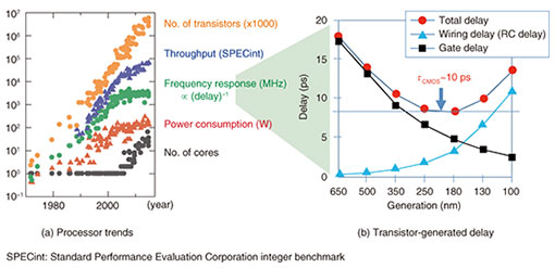
1. Importance of ultralow latency operationsImprovements are still being achieved in the processing capacity of processors by increasing the number of cores and enhancing parallelization. However, the frequency response has leveled off, as one can see in Fig. 1(a) [1]. In other words, basic throughput continues to improve through integration and parallelization, but reductions in latency or delay have reached a plateau. Particularly in situations requiring spinal reflexive speed response, this calls for a significant technological breakthrough in the development of arithmetic processors capable of responding at super high speed.
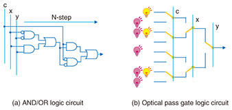
2. Introduction of optical technology in arithmetic chipsResearch and development in optical computing focused on achieving ultrahigh-speed calculations exploiting the immense broadband of light continued throughout the 1980s. The problem with this approach is that optical transistors are quite large and vastly inferior to complementary metal oxide semiconductor (CMOS) transistors in density, power consumption, cascadability, and other factors. It is not surprising that research in this area fell off sharply in the 1990s. At the same time, however, optical communications has proven vastly superior not only for long-haul communications but also in ongoing research to exploit the vast bandwidth of light in developing optical interconnects within and between chips. Today we see a marriage between light and electronics—optoelectronics—that exploits light for information transport and electronic circuitry for information processing. More recently we have seen remarkable progress in nanophotonic technology as new solutions have been found dealing with problematic issues that plagued optical and optoelectronic computing research in the past. In photonic crystal technology, for example, optical elements have been significantly downscaled to a mere 1/1000th the size they were a decade ago with corresponding decreases in power consumption, which brings optical elements into close competition with CMOS circuits. It is time that we reconsider the prevailing division between optical and electronic, with optical used primarily for transport and electronic for information processing. 3. Arithmetic chip delay factorThe frequency response rate-limiting issue mentioned earlier can be attributed to resistance (R) and capacitance (C) in the wiring path of CMOS circuits. The gate switching time of CMOS transistors has been sharply reduced by advances in semiconductor micro-fabrication technology, but the total delay of CMOS gates levels off at around 10 ps due to R and C in the transistor interconnects, as shown in Fig. 1(b) [2]. Moreover, R and C in the wiring only increases as transistors become more compactly integrated and wiring is stretched thinner and longer, which further increases the latency of actual circuits. Electronic circuits also inevitably exhibit a certain amount of latency due to their structure. One of the most widely used circuit configurations is the AND/OR logic circuit shown in Fig. 2(a). The output signal from one logic gate drives the following logic gate, so obviously, the latter gate cannot do anything until the output signal from the previous gate arrives. The wait time involved in these gate operations is proportional to the number of gates, which makes for substantial arithmetic delay.
4. Arithmetic chip with optical and electronic elements integrated at transistor levelOne solution to wiring-induced latency is on-chip optical communications. This is essentially a photonic technology for conveying information between cores, but here we extend this approach to the transistor level as a solution to the architecture-induced latency problem. In trying to come up with the ideal circuit configuration, we can find a valuable clue in the field of electronics. A schematic pyramid-shaped tree circuit based on a binary decision diagram (BDD) [3] is shown in Fig. 2(b). We assume a configuration in which “1” is output from the signal source located in the leaf part of the tree at the base of the pyramid, and Boolean operations are performed by selecting either signal source “1” or no signal source “0” depending on the combination of external inputs (x1, x2…). Various methods for simplifying BDDs have been proposed, and if these methods can be applied to the BDD-based circuit, the number of switches could be greatly reduced. This type of circuit configuration is called a pass transistor logic circuit. The signal passing through the circuit is called a carry, and an operation is performed by steering the carry flow with 2 × 1 switches. Here, we refer to the optical version of this structure as an optical pass gate logic circuit, and we replace the electronic switches with 2 × 1 and 2 × 2 optical gates. In this architecture, light is used as the carry signal. The optical pass gate logic circuit has a number of significant advantages:
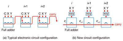
One might assume that this configuration could be just as easily implemented with electronic circuitry, but the carry signal passes right through the series resistance of multiple transistors, which would drive up R and make it virtually impossible to fabricate a high-speed response circuit. In contrast, our optical carry scheme is independent of R and C, so the carry propagation time is dramatically reduced by exploiting nanophotonic technology. For example, the propagation time for an optical gate length of 100 μm is on the order of ~1 ps. This is just a fraction of the latency generated by a CMOS gate. 5. Ultralow-latency optical parallel adderLet us consider a specific circuit configuration as an example of a digital adder. A typical electronic circuit configuration is illustrated in Fig. 3(a). The carry signal (ci) operates the gate in the i + 1th logic block, and the result generates the next carry signal (ci + 1). One will note that a certain amount of wait time is generated for the gate operations in the various logic blocks by this step. The new circuit configuration we propose is shown in Fig. 3(b). In this scheme, all gates in the logic blocks are operated collectively, and this fundamentally changes the structure of carry signal propagation.
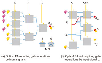
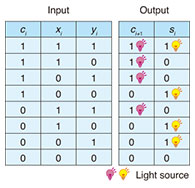
Let us first configure a BDD-based full adder (FA) as the i + 1th logic block. An FA takes two 1-bit inputs (x and y) representing the two significant bits to be added. In the circuit shown in Fig. 4(a), a Mach-Zehnder interferometer (MZI) is incorporated as a 2 × 1 switch. The switch is configured to select the upper (lower) input port when the input signal (xi, yi, ci) is “1” (“0”). The circuit selects the light source located in the leaf part of the tree structure according to the truth table in Table 1. Note that xi, yi, and ci are all input at the same time, and consequently, all the MZIs are driven at the same time. This allows the carry operation [ci + 1 = CARRY (xi, yi, ci)] and ith digit addition [si = SUM (xi, yi, ci)] to be completed just by propagation of light from the light source.
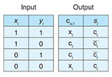
Note, however, that this circuit only adds two 1-bit inputs, x + y. In order to add multi-bit inputs, the optical carry signal (ci + 1) output from the ith FA circuit must be capable of operating the i + 1th FA circuit gate. For example, this could be achieved using an optoelectronic (OE) converter. Although there is a way of converting ci + 1 to electronic signals, this involves latency, which again raises the issue of delayed operation time. This led us to implement the block diagram shown in Fig. 4(b) [4]. This circuit operates according to the truth table in Table 2, which redefines the truth table in Table 1. Instead of the light source in Fig. 4(a), here we employ optical ci and xi signals. Light ci uses output from the ith FA circuit, while the optical xi signal is produced by combining light from the light source and from the MZI in the upper left. As is apparent from Table 2, the CARRY and SUM operations respectively select ci (xi) and
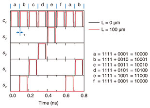
The simulation results for 4-bit addition are presented in Fig. 5. The leading edge of each digit’s signal reveals the response speed of XOR operations. Note that arithmetic latency of XOR does not accumulate as the number of digits increases. However, τ in the figure reveals a cumulative arithmetic delay of four digits, which generates a delay of about 1 ps per digit using a 100-μm-long MZI. The bottom line is that this ultralow latency figure is far smaller than the 22-ps-per-digit latency of current state-of-the-art circuits implemented in CMOS.
6. Future prospectsThis article introduced ultralow-latency optical pass gate logic circuits using a digital adder as an example. We plan to build on this new architecture as we pursue operational trials on ultrasmall-feature devices that we are now developing as a concurrent project. References
|
||||||||||