|
|||||||||||||||||
|
|
|||||||||||||||||
       |
Regular Articles Vol. 16, No. 10, pp. 60–70, Oct. 2018. https://doi.org/10.53829/ntr201810ra1 High-accuracy SS-OCT Thickness Measurement Using Refractive Index Dispersion AdaptationAbstractSwept-source optical coherence tomography (SS-OCT) is a technique to capture tomographic images of moving samples at high speed with high resolution at the level of several tens of micrometers. We have developed highly precise thickness measuring instruments used in factory automation by using the SS-OCT technique based on a KTa1−xNbxO3 (potassium tantalate niobate) deflector, which is an optical switch device used for optical communication. However, since the principle of SS-OCT is to measure the time the light reciprocates in the sample (by converting it to the frequency of the beat signal between the reference light and the sample reciprocating light), there is a problem in that the thickness measurement value of the sample varies depending on the wavelength of light due to the refractive index wavelength dispersion of the sample. To solve this problem, we modified the beat signal according to the dispersion of the sample by signal processing. As a result, we confirmed that fluctuation of the thickness measurement value was suppressed even when using light of different wavelengths. Keywords: SS-OCT, thickness measurement, refractive index dispersion
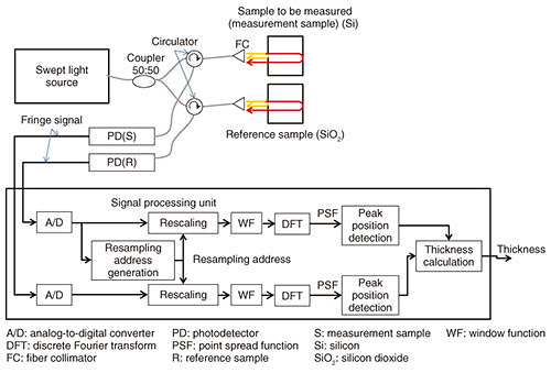
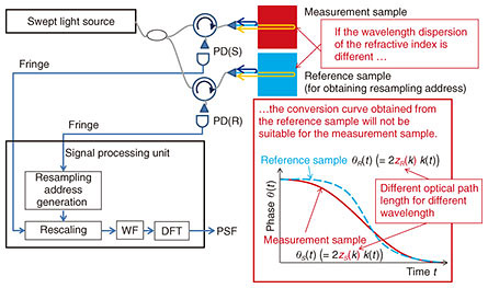
1. IntroductionIn factory automation, measuring in real time whether products meet specifications is important for efficient product manufacturing. We have developed a high-speed thickness measuring instrument for this purpose using optical coherence tomography (OCT) [1, 2] by applying optical communication technology, specifically, high-speed optical switching using a potassium tantalate niobate (KTa1−xNbxO3, or KTN) light deflector [3, 4]. OCT is a technique for producing tomographic images with a resolution of several tens of micrometers. The technique is useful for cell-level diagnosis and has been put to practical use as a biological tomographic imaging apparatus for medical use. There are two types of OCT: time domain OCT (TD-OCT) and Fourier domain OCT (FD-OCT). In addition, swept-source OCT (SS-OCT) has been attracting attention. It is a variation of FD-OCT, which is advantageous in that it enables the acquisition of tomographic images in real time. SS-OCT uses a wavelength swept laser as a light source, which is a laser that continuously varies (sweeps) in wavelength with time. SS-OCT operates in two steps. First, the SS-OCT apparatus produces interference between two light waves—reflected light (sample light) obtained by irradiating light to the sample to be measured (measurement sample) and light (reference light) that passes through a fixed length optical path. Next, frequency analysis is performed on the intensity signal (interference signal) of the interfered light to obtain depth information on the sample. Since the frequency of the interference signal is proportional to the optical path difference between the optical paths through which the sample and the reference light pass, it is possible to measure the position of the reflection point in the sample by analyzing the frequency. In our thickness measuring instrument, reflected light beams from both the back and front sides of the measurement sample are respectively used as sample and reference light beams. (That is, the sample itself functions as a Fabry-Perot interferometer.) At this time, since the combining of the sample and the reference light is performed on the sample front side surface, the optical path length difference is twice the product of the thickness and the refractive index of the sample. Therefore, since the refractive index varies depending on the wavelength due to the refractive index wavelength dispersion of the sample, there is a problem in that the thickness measurement value differs accordingly, if the central wavelength is different. To solve this problem, we use the characteristic of the refractive index wavelength dispersion of the sample to correct the interfered light signal according to the difference in the center wavelength. As a result, we confirmed that the fluctuation of the thickness measurement value was suppressed [5]. 2. SS-OCT thickness measurement instrumentThe basic construction of our thickness measurement instrument using the SS-OCT technique is shown in Fig. 1. The thickness of a reference sample is already known, and the thickness value is used as a reference value for thickness measurement.
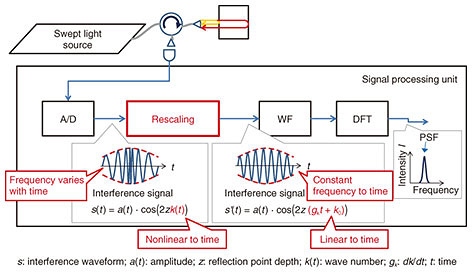
The light wave of the swept light source is divided into two light waves by a coupler and irradiated to the measurement sample and the reference sample via the circulator (C) and the fiber collimator (FC), respectively. As described above, each sample functions as a Fabry-Perot interferometer, and the light wave irradiated to each sample is reflected on the front surface and the back surface of each sample, and light waves from the front and back surface are multiplexed on the front surface of each sample to become the interfered light wave. The interfered light of the measurement sample and the reference sample is input to the photodetectors PD(S) and PD(R) via the FC and the circulator and photoelectrically converted. The signal obtained by converting the interfered light into an electrical signal is called an interference signal. The interference signal generated by the measurement sample is referred to as a measurement interference signal, and the reference sample is referred to as a reference interference signal. The interference signal s(t) is generally expressed by the following equation [6], The instantaneous frequency ƒ(.) at time t of the interference signal is expressed by the following equation, If k(.) is linear with respect to time t (referred to as wavenumber linear), since k'(.) is constant with respect to time t, the interference signal frequency ƒ(.) becomes constant. Therefore, the Fourier transform result S(.) of the interference signal s(.) is as follows, 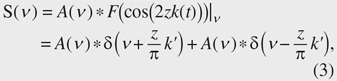 According to Eq. (3), the Fourier transform result of the interference signal is a signal in which the A(.) signal centered on zk'/π and the inverted A(.) centered on −zk'/π are arranged symmetrically around the frequency zero. Therefore, when we extract only the signal of the positive frequency and detect its center frequency νc, we can calculate the optical thickness z by z = πνcz/k'. Here, the signal centered on νc is called a point spread function (PSF). Its shape is indicated by A(.) as shown in Eq. (3). Normally, PSF is a function expressing the blurring degree of a point in an image, but in the OCT image, it represents the blurring degree of the signal representing the reflection point in the measurement sample. Incidentally, if k(t) is nonlinear with respect to time t, ƒ(t) fluctuates over time, and F(cos(2zk(t)))|ν is not a linear combination of the two δ functions. Therefore, the width of the PSF increases, and the signal representing the reflection point becomes blurred. In other words, the resolution of the OCT image deteriorates. Rescaling is one method of narrowing the width of the PSF [6]. This involves shaping the waveform of the interference signal to be linear with respect to time by sampling (hereafter, expressed as ‘resampling’) the interference signal s(t) at a specific timing to equally divide phase θ = 2zk(t), which is the argument of the cosine function of Eq. (1). Rescaling is described in detail later in the article. The sampling timing data (denoted as ‘resampling address’ in Fig. 1) in the resampling process are generated from the reference interference signal. Resampling (rescaling) is performed on both the sample interference signal and the reference interference signal using the resampling address. Each rescaled interference signal is Fourier transformed after being windowed. PSF signals are respectively obtained from the sample and reference interference signals, and their peak positions are calculated. The peak position corresponds to the aforementioned νc = zk'/π. In the thickness measurement, the thickness zS of the optical path length is measured by calculating zS = zR (νcS/νcR) using νcS = zSk'/π corresponding to the measurement sample and νcR = zRk'/π corresponding to the reference sample. The advantage of this method is that it is unlikely to be affected by the time variance of the wavelength. 3. Rescaling signal processingAn outline of the rescaling process is shown in Fig. 2. Rescaling is a process of converting an interference signal whose frequency varies with time into a signal whose frequency is constant with respect to time.
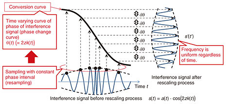
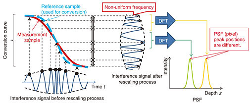
The basic mechanism of rescaling is described below. The fact that θ = 2zk(t), which is the argument of the cosine function of the interference signal in Eq. (1), does not linearly change with time is problematic in that F(cos(2zk(t)))|ν in Eq. (3) is not a sum of two δ functions. One method to effectively solve this is to resample the interference signal so that θ = 2zk(t) changes linearly with time. Let us assume that an inverse function t(k) of k(t) is obtained. (The method of obtaining t(k) is described later.) With t(k), the interference signal s(t) of Eq. (1) is resampled at times (resampling address) tn = t(δk ・ n + k0) such that the sampling point interval becomes δk (constant), and at the timing t' = nδt (δt is constant), the sample signal s(tn) is rearranged. As a result, the rearranged signal s'(t') is equivalent to the case where the wave number linearly changes to time t'. That is, k(tn) = gktn + k0, where gk = δk/δt. As described above, the frequency of the interference signal subjected to rescaling processing is constant with respect to time. In the above description, the method of acquiring the resampling address using wavenumber k of light is shown, but the address can be similarly obtained even by using the phase θ = 2zk(t). In the actual processing, phase θ(t) can be directly calculated as described later, so the resampling address is calculated using phase θ(t). A diagram of the concept of rescaling is shown in Fig. 3.
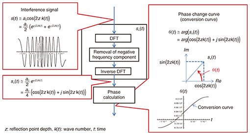
When the interference signal s(t) is resampled with sample points (resampling address) having equal phase intervals with respect to the phase change curve, s(t) is converted into an interference signal s'(t') whose frequency is constant regardless of time. Hereinafter, the phase change curve is referred to as the conversion curve. For rescaling, t(θ) needs to be known before rescaling. For this purpose, it is necessary to find θ(t). Therefore, a specific method for obtaining θ(t) is described below. When the optical distance of the thickness of the measurement sample shown in Fig. 1 is z, the interference signal output from the PD is expressed by Eq. (1). To simplify the explanation, the interference signal s(t) is simplified as follows by assuming a(k(t)) is constant over time, 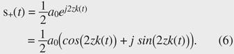 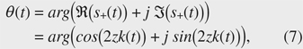 An example of the signal processing procedure for obtaining the conversion curve θ(t) from the interference signal s(t) is shown in Fig. 4. To obtain s+(t) from s(t), s(t) is Fourier-transformed, the negative frequency component is removed, and inverse Fourier transform is performed. Then, θ(t) is obtained by calculating the argument of s+(t). By obtaining t(θ) from θ(t), obtaining the sampling address having the constant interval δθ from t(θ), and sampling the interference signal using the sampling address, we can obtain an interference s'(t') equivalent to that obtained when a wavenumber linear swept light source is used. Since θ(t) and k(t) can be used in the same way to obtain the sampling address, k(t) may be used instead of θ(t). If z is known, k(t) is obtained from θ(t) as follows,
4. Problem of rescaling signal processingIn our thickness measurement instrument as shown in Fig. 1, the reference sample to acquire the resampling address and the measurement sample (sample to be measured) are different. From the viewpoint of wavelength dispersion, it is desirable that the measurement sample and the reference sample are made of the same material. However, in order to acquire a highly accurate resampling address from a signal with a high signal-to-noise ratio, since the measurement sample and the reference sample cannot be made of the same material when the light transmittance of the measurement sample is low, the reference sample material should have high transmittance, unlike the measurement sample. We show in Fig. 5 a diagram extracted from Fig. 1 of the process to obtain the PSF of the measurement sample of the thickness measurement instrument. If the wavelength dispersion of the refractive index of the measurement sample and that of the reference sample are different, the ratio zS(λ)/zR(λ) of the optical path lengths in two samples will differ with wavelength. Therefore, the conversion curve θR(t)(= 2zRk(t)) obtained from the reference sample will not have a similar shape to the conversion curve θS(t)(= 2zSk(t)) adapted to the dispersion of the measurement sample.
The effect on the PSF position when the conversion curve is not appropriate is shown in Fig. 6. When the conversion curve used for generating the resampling address is not suitable for the measurement sample, even if the rescaling is performed, the frequency of the interference signal will not become uniform with respect to time. For this reason, the peak position of the PSF will vary depending on the area of the interference signal on which Fourier transform is performed. Similarly, when the sweeping wavelength band of the swept light source is shifted, the peak position of the PSF shifts.
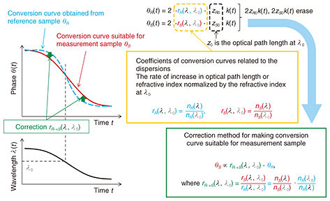
5. Correction method of conversion curveSince the shift in the PSF peak position described above is caused by the fact that the conversion curve generated in the reference sample does not match the measurement sample, it is necessary to correct the conversion curve generated using the reference sample so that it fits the measurement sample. An outline of the conversion curve correction is shown in Fig. 7. The phases θR(t) and θS(t) of the interference signals of the reference sample and the measurement sample are given below,
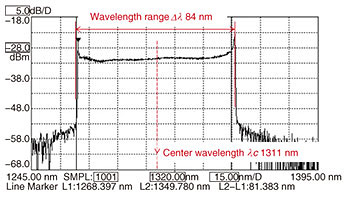
To convert the conversion curve θR(t) obtained from the reference sample into a conversion curve suitable for the measurement sample, we use the method described below to make θR(t) similar to θS(t) by multiplying θR(t) by the correction coefficient (expressed as rR→S(λ, λ0)). At this time, θR(t) and θS(t) have the following relationship, Incidentally, before calculating θR'(t), it is necessary to obtain λ(t) in order to calculate the product of rR→S(λ, λ0) and θR(t). It is likely to be calculated as λ(t) = 4πz/θ(t) in consideration of Eq. (8), but since z is a function of wavelength λ because of the effect of the refractive index wavelength dispersion, it is difficult to obtain λ(t) analytically from the following formula with z in Eq. (8) as a function of λ, 6. Experimental results and discussionIn the experiment, silicon (Si) was used as a measurement sample, and fused quartz glass (silicon dioxide: SiO2) was used as a reference sample. As shown in Fig. 8, the spectrum of the swept light source used in the experiment had a center wavelength of 1311 nm and a wavelength range of 84 nm.
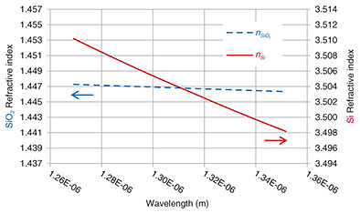
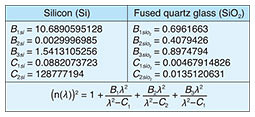
The refractive index wavelength dispersions of Si and SiO2 are shown in Fig. 9. They were approximated by the Sellmeier equation [7] using the coefficients given in Table 1. According to Fig. 9, since the rates of change of the refractive index with respect to the wavelengths of Si and SiO2 are different, these phase change curves are not similar.
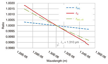
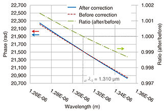
We show in Fig. 10 the correction coefficients rS(λ, λ0), rR(λ, λ0), and rR→S(λ, λ0) when λ0 = 1310 nm (1.310 μm). Further, conversion curves before and after correction are plotted in Fig. 11. The one-dotted chain line represents the ratio between them, and we can see that the conversion curve is corrected with reference to 1310 nm.
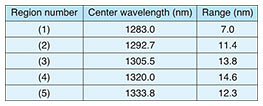
The relationship between the center wavelength and the thickness of the measurement sample was investigated to confirm whether the deviation of the thickness measurement value due to the wavelength shift improves by correcting the wavelength dispersion. Specifically, the wavelength region was divided into five regions, and then the PSF was calculated and the silicon thickness was measured for each region. The center wavelength and region for each of the five regions are listed in Table 2. To clearly observe the suppression of fluctuation in the thickness measurement value with respect to wavelength fluctuation, the difference between the center wavelengths of regions (1) and (5) is relatively large at about 50 nm.
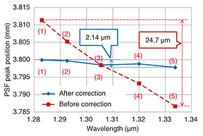
The results of measuring the thickness of Si as the measurement sample are shown in Fig. 12. Before the correction of the conversion curve (wavelength dispersion non-adaptive), the measured value shifted by 24.7 μm with respect to the deviation of the central wavelength of 50 nm. After the correction (wavelength dispersion adaptation), however, it only shifted by 2.14 μm. This result indicates that the deviation width of the thickness measurement value was improved to a width that was about one-tenth of that before correction.
7. SummaryWith the SS-OCT thickness measuring instrument, if the refractive index wavelength dispersion of the sample to be measured is not taken into account, a deviation will occur in the thickness measurement value due to deviation of the central wavelength of the light source. To solve this problem, we adapted the rescaling process to the wavelength dispersion of the sample to be measured and confirmed that the deviation of the thickness measurement value improved to about one-tenth of the value before adaptation. References
|
||||||||||||||||