|
|||||||||||||||
|
|
|||||||||||||||
       |
Feature Articles: Photonics-electronics Convergence Technology to Achieve All-Photonics Network Vol. 18, No. 10, pp. 21–30, Oct. 2020. https://doi.org/10.53829/ntr202010fa3 Device Technology for Short-range Optical Interconnections with High Density and Low Power ConsumptionAbstractOptical interconnections, which apply optical technology to short-range communications on printed circuit boards in datacenters, are being studied for faster information processing infrastructure and lower power consumption. In this article, we introduce membrane-type directly modulated lasers on silicon (Si) substrates. These lasers can be integrated with Si photonic devices and driven by complementary metal oxide semiconductor-based drivers with low power consumption. Keywords: photonics-electronics convergence, optical interconnection, semiconductor laser diode
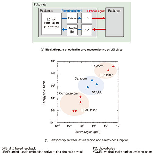
1. IntroductionDue to progress in the Internet of Things and expansion in the use of artificial intelligence, a huge amount of data has been handled, exceeding our expectations, and this trend is expected to continue. It is estimated that the power consumption of information and communications equipment will increase at an accelerated rate as a result of this increase in data processing [1]. If traffic continues to increase and the performance of information and communications equipment does not change, it is predicted that information and communications equipment in 2030 will consume nearly twice today’s annual power consumed in Japan. In particular, locations of data processing tend to be concentrated in large datacenters, and the power requirements for datacenters are becoming more stringent at an accelerating data rate. For example, the total power consumption of datacenters in Japan was estimated to be 1% of the annual power consumption in Japan in 2015; thus, it is important to reduce the power consumption for data processing and transmission. NTT proposed the concept of the Innovative Optical Wireless Network (IOWN) with ultralow power consumption. To achieve this, we are conducting research and development (R&D) on photonics-electronics convergence technology to apply devices used for long-distance communications to short-distance communications. Optical communication technology has been applied to international long-distance communications and domestic metro access networks and has recently been applied to communications between datacenters and between racks and printed circuit boards in datacenters. Electrical wiring, however, is used for communications on such boards and between large-scale integrated circuits (LSIs). The transmission loss increases with the increase in data rate and transmission distance. Optical wiring, on the other hand, is characterized by an almost constant transmission loss and small increase in power consumption while increasing the data rate. NTT is conducting R&D on optical interconnections that apply optical technology to short-range communications on printed circuit boards in datacenters to increase the speed and reduce power consumption of electronic devices used for data processing and transmission. 2. Device technology for short-range optical interconnectionsFigure 1(a) shows a block diagram of optical interconnection required for information processing. Optical transmitters and receivers are placed in the vicinity of LSIs to convert electrical signals into optical signals. High-density integration and low power consumption of optical devices, such as semiconductor laser diodes (LDs), are essential to apply optical communication technology to shorter distances. Figure 1(b) shows the relationship between the size of the active region and energy consumption of directly modulated LDs used at various distances. In general, when we use LDs with larger active region, larger optical output power can be obtained, although energy consumption is also increased. In telecommunication, large optical power is required for long-distance transmission, and LDs with large active regions are required. The need to reduce energy costs is increasing for data communications such as inter-board transmission. Vertical cavity surface emitting lasers (VCSELs), which are the most widely used light sources in current short-distance communications, tend to oscillate in multiple modes because of their shape and are not suitable for wavelength division multiplexing (WDM) technology. To increase the transmission capacity, it is necessary to integrate single mode LDs and a wavelength multiplexing circuit. Although VCSELs can shorten the cavity length, which determines the active region, there is a limit to the miniaturization of the active region. NTT is developing thin film (membrane) directly modulated LDs fabricated on silicon (Si) substrates as light sources for on-board optical interconnections. By fabricating LDs on Si substrates, Si photonics technology can be applied to integrate WDM circuits and photodiodes at high density and low cost. In addition, by fabricating LDs on silicon dioxide (SiO2) layers that have a low refractive index, the LDs can be miniaturized. We can reduce power consumption with this structure owing to the large interaction between light and injected carriers. We are also developing wavelength-scale cavity LDs using photonic crystals to fabricate LDs composed of even smaller active layer regions since the energy consumption of a directly modulated LD is proportional to the size of the active region.
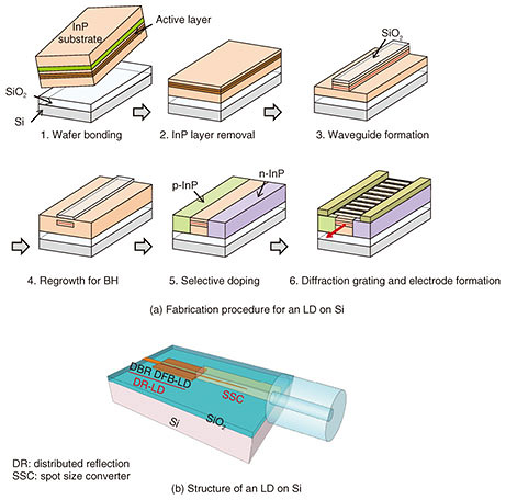
In the following sections, we describe the fabrication and characteristics of LDs on Si substrates and driver circuit design using complementary metal oxide semiconductor (CMOS) technology. We also explain an LD using photonic crystals as our approach for further reducing the power consumption of LDs. 3. Thin film on Si substrate (membrane) directly modulated laserFigure 2(a) shows the fabrication procedure of an LD on Si substrate [2]. First, optical circuits are formed on Si substrates using Si photonics technologies, then the indium phosphide (InP)-based active layers are bonded to the SiO2/Si wafer. The active layers consist of indium gallium aluminum arsenide (InGaAlAs)-based multiple quantum wells (MQWs). Mesa stripes are formed by masking the LD regions and etching MQWs. An undoped InP layer is selectively regrown using a metalorganic vapor phase epitaxy to fabricate InGaAlAs/InP buried heterostructures (BHs), which are island-like active layers embedded in thin InP. To inject current into the BHs, n-type and p-type doping regions are formed on either side of the BHs using Si ion implantation and zinc (Zn) thermal diffusion. This structure has advantages in both optical and carrier confinement into BHs. Large optical confinement is achieved owing to the large refractive index contract between the InP and the SiO2 cladding. Carrier confinement is achieved due to the electrical bandgap difference between the MQWs and surrounding InP that has a bandgap larger than the MQWs. These characteristics make it possible to reduce the size and power consumption of LDs on Si compared to conventional LDs fabricated on InP substrates. The structure of a fabricated LD on Si is shown in Fig. 2(b). The laser-cavity structure is a distributed reflection type that has a distributed Bragg reflector (DBR) on the rear side of the distributed feedback region. The rear DBR allows the lasing light to be selectively emitted from the front of the LD, making the BH smaller. On the front side of the LD, we integrated spot size converters using a SiOx waveguide, enabling efficient optical coupling with optical fibers.
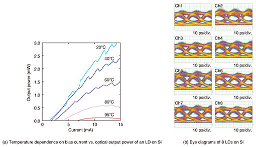
Figure 3(a) shows the injected current versus optical output power of the fabricated LD. We obtained continuous-wave operation at room temperature with a threshold current of 1.6 mA and lasing wavelength of 1.3 μm. Continuous-wave operation was possible up to 95ºC. Figure 3(b) shows eye diagrams of eight LDs integrated on the same wafer. The bit rate was 25.8 Gbit/s with the non-return-to-zero (NRZ) format. The energy consumption of a single LD was 200 fJ/bit, which was on the same order of that of VCSELs. WDM circuits can also be integrated monolithically with the same structure [3].
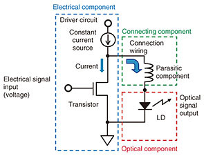
We were successful in fabricating membrane LDs as low-power-consumption light sources that can provide single-mode lasing and have excellent capability for monolithic integration. 4. CMOS driver circuit technologyThis section describes the electrical circuits used to drive the LDs. An LD needs to be driven by an electric current to emit light. However, general digital electric circuits, such as LSIs, operate with voltage as a signal, so a driver circuit is required to convert voltage signal into current. The optical transmitter shown in Fig. 4 consists of an electrical component (the driver circuit), optical component (LD), and connecting components such as the wiring. This circuit operates as follows. The current from the constant current source is branched (shunt) to flow to either the transistor side or LD side. At this point, when a high-speed electrical signal is input from the left side using a voltage, the transistor acts as a switch and turns on/off. Since the constant-current source continues to supply a constant current, a current flows to the transistor side when the transistor is turned on. Less current flows to the LD side, and no light is emitted. When the transistor is turned off, however, current flows to the LD side, and light is emitted. Therefore, the light emission of an LD can be turned off and on by turning on and off the transistor.
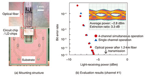
The requirements for driver circuits are high-speed operation, low power consumption, and small size. To meet these requirements, we selected CMOS technology to fabricate the transistors and applied our core opto-electronic integrated design technology [4] to the electrical circuits. It was necessary to fabricate a prototype of the optical transmitter, measure the characteristics of the electrical and optical components, and redesign to tune the parameters of the components. With our opto-electronic integrated design technology, we constructed a model in which the optical and connecting components are replaced with an electric equivalent circuit. By incorporating this model into the field of electrical circuitry where simulation and design tools are mature, it is possible to make performance predictions through integrated design. Next, we describe a small mounting structure of the optical transmitter (Fig. 5(a)). For the electrical connection, the surface of the CMOS driver circuit chip is mounted on the surface of the LD chip. This not only reduces the chip area but also shortens the electrical-wiring connection, reducing the parasitic inductance and allowing high-speed signals to pass through. For optical connections, we connected a 4-channel optical fiber array directly to the end facet of the LD chip with a width of 1 mm, enabling small and low-loss optical connections. The characteristics of the optical transmitter are shown in Fig. 5(b) [5]. A pseudo random bit string (7 steps) with a bit rate of 25 Gbit/s NRZ is input to each channel, and the transmitter consists of 4 channels to achieve a transmission capacity of 100 Gbit/s. The inset shows the eye diagram of the optical signal output from one channel, and we obtained an eye opening with an extinction ratio of 3 dB or more. As a result of evaluating the bit error rate after propagating a standard single mode fiber of 1.2 km, we confirmed that error-free transmission (bit error rate < 10–12) can be achieved even when four channels are simultaneously driven. Since the total power consumption of the optical transmitter is 267 mW, the power efficiency is 2.67 pJ/bit, and low power consumption was achieved.
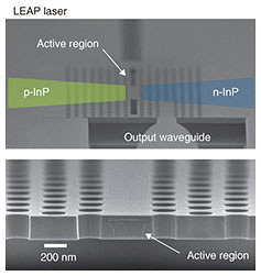
5. LEAP lasersAs explained in Fig. 1(b), further reduction in energy consumption is required for interconnection on printed circuit boards and between chips, and LDs with small active area are required. NTT developed small LDs using photonic crystals [6]. Figure 6 shows scanning electron microscopic images of one of these LDs. Photonic crystals are artificial periodic structures, and the periodicity of refractive index is the same as the wavelength of light. This structure allows the light to be localized very strongly in the designed region. We fabricated these LDs with an active layer embedded in an InP photonic crystal by using BH technology. We call these LDs lambda-scale embedded active region photonic crystal (LEAP) lasers because of their structure.
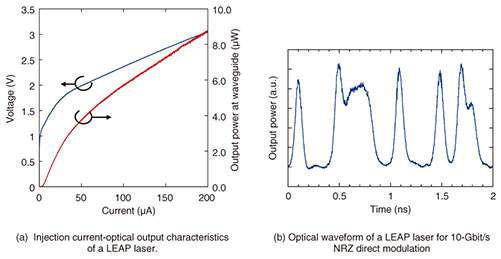
Figure 7(a) shows the injection current versus optical output power of a LEAP laser at room temperature. Even with such a small LD, we achieved continuous-wave operation at room temperature and a record low threshold current of 4.8 μA. Figure 7(b) shows a direct modulation waveform with an NRZ signal of 10 Gbit/s at a bias current of 25 μA. Direct modulation was possible even with such a small bias current, and a record low-energy consumption of 4.4 fJ/bit was achieved with a single LD.
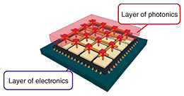
Therefore, we demonstrated that power consumption can be much lower with LEAP lasers. LEAP lasers can be formed not only on InP substrates but also on Si substrates by combining them with the bonding technology described in the previous section. 6. Future developmentsThe semiconductor LDs on Si substrates introduced in this article can be integrated with Si photonic devices and driven with low power consumption by using a CMOS driver. We will continue to strive for higher transmission capacity and higher density integration and further advance integration with information processing circuits such as in central and graphics processing units (Fig. 8). We will also conduct further research and development to contribute to the development of future information processing infrastructure.
References
|
||||||||||||||