|
|||||||||||
|
|
|||||||||||
|
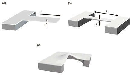
Feature Articles: The Forefront of Nanomechanics Research Vol. 20, No. 4, pp. 32–36, Apr. 2022. https://doi.org/10.53829/ntr202204fa5 Nanomechanics: Outline and Future ProspectsAbstractMicroelectromechanical systems (MEMS) technology, which uses the mechanical motion of miniaturized structures artificially fabricated on a chip, has been used in various fields such as mobile communications and Internet-of-Things devices. This article introduces the concepts and future prospects of nanomechanics technology, which further extends the functionalities from MEMS technology, focusing on research activities conducted at NTT laboratories. Keywords: nanomechanics, phonon, nanotechnology  1. What is nanomechanics technology?What do you imagine when you hear the word “nanomechanics”? The term “nanotechnology” has been used for a long time, so I think many people know that “nano” refers to a very small object. The origin of this word is the unit “nanometer (nm),” which represents an extremely small size of one billionth of a meter. Such minuteness is not easy to imagine, but, to put it into perspective, atoms range in size from only about 0.1 to 0.2 nm. The next unit is “micrometer (μm),” which is one millionth of a meter, and nanotechnology deals with sizes ranging from about 1 nm to 1 μm. Incidentally, the novel coronavirus that has caused the COVID-19 pandemic is about 100 nm, so it falls within the size range of this technology. What does “mechanics” mean? The first thing that comes to mind when we hear “mechanics” is possibly Newtonian mechanics, which led to the discovery of gravitational force through the observation of a falling apple. It describes the relationship between the motion of an object (apple) and the force applied to it. Therefore, nanomechanics is a field of study focused on the relation between the force applied to objects and their motion in the extremely small world represented by the size of viruses. The nanomechanics we are studying is an attempt to develop technology that uses the physical laws governing such small force and motion. Forgetting about the microscopic world for a moment, imagine a temple bell. The bell makes a sound because the metal that makes up the bell causes periodic elastic vibrations. This behavior can also be accurately described using the laws of physics. If the vibration is repeated 440 times per second, the sound has the frequency of 440 hertz (Hz). This corresponds to the reference pitch “la” in the C-major scale used in music. The frequency of 523.23 Hz produces a slightly higher “do” sound, and 783.98 Hz produces a higher “so” sound. The faster the vibration, the higher the sound frequency, so it is easy to imagine that the smaller the bell is, the higher the frequency will be. Therefore, a nanometer-sized bell will vibrate at a very high frequency. This is the essence of our research; namely, we are using cutting-edge microfabrication technology to create extremely small “bells” and developing a technology that uses their high-frequency vibrations. 2. Nanomechanical oscillatorOf course, making a submicrometer-scale structure with the shape of a temple bell is not straightforward with present microfabrication technology. We therefore use simpler structures that are easier to make. Figure 1 shows typical examples, where Fig. 1(a) is a structure called a cantilever. It is just like a diving board at a swimming pool, and it vibrates when you hit the edge. The structure in Fig. 1(b) is called a doubly clamped beam, and it is shaped like a bridge. Both ends of the beam are supported, so setting into vibration is harder than it is for a cantilever, and it has a higher vibration frequency. Both structures are thin and plate-like in shape, but their cross sections can have other shapes. The nanomechanical oscillator reported in the Feature Articles in this issue has a cylindrical or hexagonal cross-sectional shape of several hundred nanometers in diameter, which is produced by crystal growth. Figure 1(c) is a circular membrane oscillator, which acoustically vibrates like a drum. In this issue, we also describe a nanomechanical device called a phononic crystal waveguide, which guides and transmits elastic vibrations to form an acoustic circuit. In this waveguide, a number of membrane oscillators are connected with equal spacing.
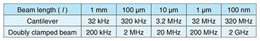
Table 1 shows how the frequencies of the cantilever and doubly clamped beam change with the structure size calculated for a typical semiconductor, gallium arsenide (GaAs). Even with the same shape, the doubly clamped beam has about a six times higher frequency than the cantilever. When its length is 100 nm, the frequency enters the gigahertz range. Gigahertz (GHz) is the frequency of the radio waves used for mobile phones, and it is 100,000 times higher than that of highest sound we can hear, which is about 10 kilohertz (kHz). Therefore, by using nanomechanical structures, it will be possible to develop a technology that can control acoustic vibrations at extremely high frequencies, called ultrasonic waves or extreme ultrasonic waves. Focusing on this unique feature of nanomechanical oscillators, we have been researching nanomechanics for nearly 20 years. The frequencies we are studying cover the range from around 100 kHz to 1 GHz, but, in this issue, we mainly introduce our research activities in the relatively low frequency range of up to 10 megahertz (MHz).
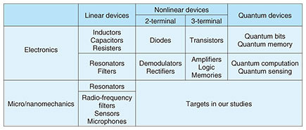
3. Applications of nanomechanicsMicroelectromechanical systems (MEMS) are being widely and actively studied for using such elastic motion of an artificial structure. Our research uses two unique approaches to extend the device functionalities in MEMS technology. The first is to use the nonlinearity of the elastic properties. “Nonlinearity” may be an unfamiliar word, but consider that common semiconductor devices such as diodes and transistors have demonstrated a variety of functions due to nonlinearities. These functions cannot be found in devices with only linear characteristics such as inductors, capacitors, and resistors. By harnessing nonlinear characteristics, we aim to create mechanical devices with innovative functions similar to those of diodes and transistors. The other approach is to create new functions by combining functional materials such as semiconductors and optical materials. Such materials, which have thus far been used in electronic and optical devices, can also be applied to mechanical devices to create new principles by combining the optoelectronic function with elastic vibration. By incorporating nanostructures known as quantum nanostructures, it is possible to apply such mechanical devices to quantum technologies, which are attracting much attention (Table 2).
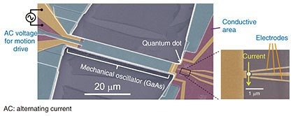
Figure 2 shows an electron micrograph image of a quantum-sensor device as an example of quantum nanomechanical technologies. A quantum dot is embedded at one of the two clamping areas of the beam structure, making it possible to detect elastic vibration with ultrahigh sensitivity. Vibrations of 0.1 picometers (ten trillionths of a meter), corresponding to the diameter of an atomic nucleus, can be detected through current measurement. This electromechanical device makes it possible to detect displacement caused by extremely small forces applied to the beam, thus to use it as an ultrasensitive acceleration, magnetism, molecular, and atom sensors.
In the Feature Articles in this issue, we introduce five topics on which our group has made significant progress. First, as an example of nonlinear nanomechanics, we introduce a new method for generating chaos [1]. Chaos used to be regarded as random and uncontrollable behavior, which was considered an obstacle to its application. However, in the field of machine learning, this chaotic behavior is expected to play an important role in improving learning efficiency. Secure communications using chaos has also been proposed, so how to accurately control the chaos generation is now an important research subject. As the second topic, we introduce phonon waveguides using phononic crystals [2]. The term “phonon” is used in a sense similar to “photon” for light or “electron” for electric current. A phonon is a sound particle that is the basic unit of elastic vibration. We developed a method of controlling the flow of phonons using nonlinearity. This research demonstrated a phonon transistor for the first time, which controls the propagation of sound waves in a way similar to how a transistor controls the electron flow in circuits. This device is expected to play a central role in phononic integrated circuits, where a large number of nanomechanical devices exchange acoustic signals. The third topic is a new optomechanical device using a rare-earth element, which is a functional material widely used in fiber optics [3]. Optomechanics is a technology that combines the functions of both light and mechanics, and is one of the technological fields in which research has been making great progress. Rare-earth elements, such as erbium, are materials that absorb and emit light in the telecom wavelength bands and can be widely used in optical communications and quantum technologies. In this issue, we report on a new method of mechanically controlling light emission from erbium atoms by incorporating them into a cantilever. The fourth topic covers the detection of the mechanical vibration of a semiconductor nanowire with high sensitivity by using a unique optomechanical setup [4]. Semiconductor nanowires are self-organized nanostructures produced by crystal growth. Since no microfabrication method such as lithography is used for forming their three-dimensional shapes, the structures have high crystalline quality. In addition, it is possible to incorporate heterostructures, which are used in semiconductor lasers, high-speed transistors, and various quantum structures—the key elements in optoelectronic and quantum technologies. By using nanowires as nanomechanical structures, it is expected that advanced functions achieved by combining electronic, optical, and quantum devices will be incorporated into mechanical devices. The final topic is a novel fabrication method in which an inkjet-printing technique is used to fabricate nanowire mechanical devices [5]. Inkjet printing is a basic technology used in our daily lives, but we have recently seen it used as a new microfabrication technology. This section describes how inkjet printing can be used to arrange semiconductor nanowires at desired positions on a semiconductor wafer and assemble them as nanomechanical devices. 4. Future prospectsCompared with electronic and optical devices, nanomechanical devices are still in the early stages of research, and there is a possibility of significant developments in the future. NTT laboratories are conducting research to develop new information processing technologies such as machine learning, Internet of Things, and quantum technologies, where the nanomechanical devices introduced in this issue are expected to play essential roles. References
|
|||||||||||