|
|||||||||||||||||
|
|
|||||||||||||||||
       |
Feature Articles: Device Technologies for Enabling the All-Photonics Network Vol. 20, No. 8, pp. 28–34, Aug. 2022. https://doi.org/10.53829/ntr202208fa3 Development of Membrane Optical Modulators for IOWNAbstractTo develop a high-speed, large-capacity optical network with low power consumption, which is important for IOWN (the Innovative Optical and Wireless Network), we are conducting research and development on membrane optical devices that integrate III-V compound semiconductors on silicon-photonics circuits. Membrane optical devices are expected to be used for high-modulation efficient lasers and optical modulators because they can achieve high optical confinement in the core layer. This article introduces the current state of research and development focusing on optical modulators and the integration of such modulators and lasers on the basis of membrane-device technologies. Keywords: silicon photonics, optical interconnection, optical modulator
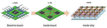
1. IntroductionOptical interconnection is a technology that is more advantageous than data communication using electricity as the transmission capacity and transmission distance increase due to the characteristics of wide band and low loss of optical fiber. This technology has been used in long-distance communication networks since the 1980s. Due to the increase in Internet traffic, the application area where optical fiber can show its superiority has been expanded to shorter-distance transmission, and optical interconnection is widely used in datacenter networks. As the number of devices connected to the Internet and the amount of traffic from devices increase, it is expected that the increase in traffic will continue. Therefore, research interests are to increase the transmission capacity where optical interconnections have already been applied and apply optical interconnection to shorter-distance transmission, as shown in Fig. 1. Specifically, optical interconnections inside the board and chip are expected to become important for improving the throughput of electronic devices such as routers and servers.
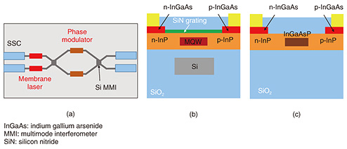
For this purpose, it is important to reduce the power consumption and cost of optical transmitters. To reduce power consumption, it is important to modulate optical devices at high speed. To achieve this, it is necessary to increase the optical-confinement factor in the core region as much as possible. A large cost is required for assembly and testing, so cost reduction is necessary by integrating multiple optical devices in the same substrate. It is therefore important to use silicon (Si) photonics technology, which can be used to fabricate optical waveguides with low loss and optical circuits with high performance by using fabrication technology used in Si electronic circuits. Since it is not possible to fabricate a laser or a highly efficient optical modulator using Si, a method for integrating III-V compound semiconductors, which are the materials for lasers and modulators, is an issue for large-scale integration. In this article, we describe membrane optical devices on Si substrates. Such devices are thin-film optical devices fabricated on low-refractive materials. We previously fabricated and demonstrated high-efficiency lasers and modulators using indium phosphide (InP)-based compound semiconductors with a typical thickness of about 250 nm on silicon dioxide (SiO2)/Si substrates [1–5]. High optical confinement of the core layer can be obtained by sandwiching a device between low-refractive index materials such as SiO2 and air. We specifically describe the optical modulators in detail. 2. Membrane optical modulatorsOptical modulators can be classified into two types: phase modulators that mainly modulate the refractive index and intensity modulators that modulate the absorption coefficient. A phase modulator is used as a Mach-Zehnder (MZ) modulator in combination with an MZ interferometer, and by combining MZ modulators and modulating the phase and intensity, it is possible to obtain a large-capacity transmission exceeding 1 Tbit/s per wavelength and long-distance transmission. Typical materials used are lithium niobate (LiNbO3), Si, and InP. Due to the increase in traffic, optical interconnects increase their importance in a datacenter. Thus, it is important to reduce the transmitter cost by reducing the device size and integrating many devices including lasers on the same chip. For this purpose, InP-based and germanium silicon (GeSi) intensity modulators, which are one order of magnitude more efficient than LiNbO3 and Si, are considered key devices. Since intensity modulators use only the intensity change as a signal, the transmission capacity is generally smaller than that of MZ modulators, but their simple and compact configuration is important when a large number of transmitters are required at shorter distances. Considering their use in the 1.3-μm wavelength used in datacenters, there is currently a problem in the growth of GeSi; thus, InP compound semiconductors have become advantageous in addition to integrate lasers. Figure 2(a) shows a schematic of a photonic-integrated circuit using an MZ modulator consisting of a Si MZ interferometer and InP phase modulators, and membrane lasers [6]. By integrating the spot size converters (SSCs), it is possible to assemble a device with optical fiber with low-coupling loss by butt-coupling the device to the optical fiber without using a lens. Figures 2(b) and (c) show the cross-sectional view of a membrane laser and membrane phase modulator. Reduction in the optical-confinement factor in the laser core layer is important to suppress internal loss and spatial hole-burning because the laser for biasing the modulator requires high output power and stable single-mode lasing. Therefore, the Si waveguide is placed under the laser core layer. Since the effective refractive index of the membrane-laser structure is similar to that of the Si waveguide, the optical-confinement factor in the laser core layer can be controlled by adjusting the width of the Si waveguide. In a phase modulator, the Si waveguide is eliminated to maximize the optical-confinement factor. Therefore, the membrane optical device can freely design the confinement of light between the Si waveguide and membrane optical device.
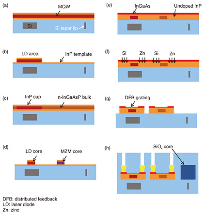
The fabrication process is shown in Fig. 3. (a) A Si waveguide is fabricated using a Si on insulator (SOI) substrate, and after the entire waveguide is covered with SiO2, it is planarized using chemical mechanical polishing, and the multiple-quantum-well (MQW) layer, which is the core layer of the laser grown on the InP substrate, is directly bonded on the planarized SiO2. (b) The MQW layer is removed by selective etching except for the area that includes the laser core layer, and the InP layer is exposed. (c) An n-type indium gallium arsenide phosphide (InGaAsP) layer, which is the core layer of the phase modulator, is grown on the InP layer by using metal organic chemical vapor deposition. (d) The laser and phase modulator core regions are formed using selective etching. (e) Core regions are embedded with an undoped InP layer by using selective regrowth. (f) Selective doping is carried out to form n- and p-type doping regions. (g) The laser and phase modulator are separated and a grating is formed in the top surface layer of the laser region. (h) Finally, an SSC and electrodes are formed. The advantage of this fabrication method involves the regrowth of compound semiconductors on Si substrates. Since the total thickness of the membrane optical device is about 230 nm, regrowth on the Si substrate becomes possible due to the resistance to the strain caused by the thermal-expansion coefficient difference between Si and InP. Thus, InP-based semiconductors with different bandgaps, such as laser-active layers and phase-modulator layers, can be fabricated on Si on a wafer scale. Since the marker for the stepper on the Si substrate is used for the alignment of the III-V core regions, the Si waveguide and membrane optical device can be integrated with the alignment accuracy of the stepper.
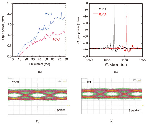
The characteristics of the fabricated device are shown in Fig. 4. The length of the laser-active region and phase modulator is 500 μm. Thanks to the high modulation efficiency of the n-InGaAsP layer, the length of the phase modulator is much shorter than the Si phase modulator, which has a length of several millimeters. Figure 4(a) shows the current dependence of the output light intensity when the MZ optical modulator is set to the OFF state. The output light is received by the lensed fiber at measurement temperatures of 25 and 80°C. In this experiment, reflection occurred at the end facet of the device, resulting in mode hopping, as shown in the figure. It is possible to suppress the reflection by directly connecting fibers, but we use lensed fiber to simplify the experiment. The threshold current was about 6 mA at 25°C and about 8 mA at 80°C. The maximum fiber output power was 2 mW at 25°C and about 1 mW at 80°C. The fiber coupling loss was 3 dB. Figure 4(b) shows the oscillation spectra at 25 and 80°C with bias currents of 76.0 and 50.6 mA, respectively. Single-mode oscillation was obtained, and the side mode suppression ratio at 80°C was 59 dB. Figure 4(c) shows the dynamic characteristics of the MZ modulator when modulated with a 50-Gbit/s non-return-to-zero (NRZ) signal at operating temperatures of 25 and 80°C. An electrical signal with a peak voltage of 2.5 V was input into the phase modulator, and the signal was terminated by 50 ohms. Although the extinction ratio was as low as 3 dB, we confirmed a clear eye-opening at both temperatures. The extinction ratio can be improved by differential operation and applying an inverted signal to the other electrode of the phase modulator. The core layer of the phase modulator is relatively long (500 μm) for lumped electrodes, but it can operate on 50-Gbit/s NRZ signals thanks to the low capacitance of the membrane structure.
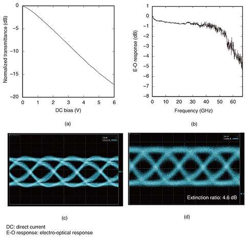
We also developed an electro-absorption modulator (EAM) using InP-based MQWs [7]. Since we can obtain large absorption change in the EAM, there is no need to use an interferometer such as an MZ modulator, which results in a very simple configuration. Therefore, EAMs with a core-layer length of about less than 300 μm on InP substrates are integrated with lasers and are widely used in datacenters. However, the operation speed of the EAM on InP substrate is limited by the capacitance, and it is necessary to use the 50-ohm termination and apply the traveling wave-type electrode to increase the speed. Therefore, the EAM using a membrane structure has attracted attention due to its low capacitance. Since it is important to increase the optical-confinement factor to the core layer as well as the phase modulator, we fabricated a device without placing a Si waveguide under the EAM core layer. A nine-layer MQW with a photoluminescence peak of 1230 nm was used as the core layer. The voltage dependence of transmittance at an operating wavelength of 1280 nm is shown in Fig. 5(a). For a device with a core-layer length of 200 μm, an extinction ratio of 8.5 dB can be obtained by changing the bias voltage from 0 to 3 V. The insertion loss of the EAM excluding the fiber coupling loss is estimated to be 3 dB compared with a Si waveguide. Figure 5(b) shows the small-signal response. The operating wavelength was set to 1280 nm, and the bias voltage was set to 2 V. We did not use a 50-ohm termination. As shown in the figure, the 3-dB band was 59 GHz. This clearly shows the advantage of a membrane photonic device. Next, we measured the eye diagrams of the 100-Gbit/s NRZ signal. Figures 5(c) and (d) show the input electrical signal and optical output signal, respectively. The bias voltage of the EAM was set to 1.2 V. An electrical signal with a peak voltage of 0.12 V from the pulse pattern generator was amplified with an electrical linear amplifier of 22 dB and applied to the EAM. The eye diagram is comparable to the input electrical signal, and the extinction ratio was 4.6 dB. Since laser integration is possible with the same manufacturing process as a MZ-modulator-integrated distributed feedback laser, it is expected to be applied to the optical interconnection of short distances such as inside racks and boards.
3. SummaryThis article argued that membrane optical modulators are suitable for fabricating modulators with high speed and low power consumption because of their high optical-confinement factor and low capacitance. An SSC is also integrated so that it can be easily connected to fiber arrays. Because an SCC can be integrated on the Si photonic circuit, it is also possible to integrate it with multiplexer/demultiplexer components using the Si waveguide. Therefore, it is expected to be a key device for short-distance optical interconnections, where it is important to integrate optical devices at high density and maximize throughput per unit length. References
|
||||||||||||||||