|
|||||||||||||||||||||
|
|
|||||||||||||||||||||
|
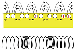
Feature Articles: Plasmon Control Technology Vol. 21, No. 5, pp. 17–20, May 2023. https://doi.org/10.53829/ntr202305fa1 Overview and Prospects for Research on Plasmons in Two-dimensional Semiconductor SystemsAbstractPlasmons, which are collective oscillations of electric charges, have a wide range of applications in sensors and other technologies. Plasmons have also been attracting attention as potential new information carriers due to their ability to be generated by light and propagate within a region that exceeds the diffraction limit of light. This article presents an overview of the research on plasmon control and basic physical properties exploiting plasmons at NTT Basic Research Laboratories. Future prospects are also discussed. Keywords: plasmonics, graphene, semiconductor  1. PlasmonsAt elevated temperatures, electrons in a gas can separate from atomic nuclei, resulting in the formation of positive and negative ions and constituting a state of matter referred to as plasma. Examples of natural plasma can be observed in phenomena such as lightning and auroras. Artificial gas plasma can also be generated through the application of high temperatures or high voltages for purposes such as welding, semiconductor processing, and nuclear fusion. Plasma can also exist in solids, derived from free electrons in metals and semiconductors. In solids, because of the high charge density, the Coulomb energy is higher than the thermal energy at ordinary temperatures, causing the behavior of solid plasma to differ significantly from that of gas plasmas. When the electron density distribution in a solid becomes nonequilibrium, an electric field is generated, and the acceleration of electrons in that field tends to restore a uniform distribution of electron density. Thus, an oscillation analogous to the longitudinal waves in a spring occurs in the charge density with overshooting and retraction due to inertia (Fig. 1). This plasma oscillation, when treated as a quantum, is referred to as a plasmon.
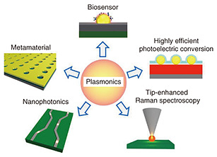
2. PlasmonicsOne characteristic of plasmons is their confinement to regions that are narrower than the diffraction limit*1 of light at the same frequency. Technology that applies this characteristic in nanoscale regions is referred to as plasmonics (Fig. 2). One example of plasmonics is in biosensors, which use the sensitivity of plasmons to the state of the metal surface in nanoparticles. Adhesion of target molecules to the metal surface causes detectable changes in plasmon frequency and attenuation. Other applications include surface-enhanced (or tip-enhanced) Raman spectroscopy, which uses the enhanced plasmon electric field in metal nanoparticles or at the tip of needles, and highly efficient photoelectric conversion. Plasmonics has also been attracting attention in nanophotonics and metamaterials. Nanophotonics deals with the conversion of light to plasmons and the control of plasmon propagation in nanoscale regions. Metamaterials deals with the design of optical properties of materials using plasmonic electric fields in periodic structures that are smaller than the wavelength of light.
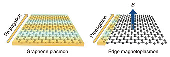
3. Plasmons in two-dimensional semiconductor systemsResearch and application of plasmonics commonly use plasmons that appear on metal surfaces. However, such plasmons have a limited application range due to significant losses and a lack of controllability. In contrast, NTT Basic Research Laboratories focuses on plasmons in two-dimensionally confined electron systems in semiconductor heterostructures and in graphene, a single atomic layer of carbon. The major advantage of two-dimensional (2D) electron systems is the tunability of plasmon characteristics through adjustment of an external electric field. This enables electrical control of plasmon properties. Since the Coulomb interaction in semiconductors is weak compared with metals due to the lower electron density, plasmons in a 2D electron system propagate at a slower velocity with a shorter wavelength, akin to compression waves in springs with a weak spring constant. The tunability and tighter confinement resulting from shorter wavelength make 2D electron systems ideal for applications in which metal surface plasmons are not feasible. Furthermore, application of a magnetic field perpendicular to the 2D plane generates edge magnetoplasmons, which are unique plasmons that propagate in one dimension along the edge of the electron system (Fig. 3).
4. Research initiatives by NTT Basic Research LaboratoriesResearch at NTT Basic Research Laboratories approaches plasmons in 2D electron systems from both applied and fundamental science perspectives. Specifics are explained in the respective Feature Articles, and a brief overview is given here. 4.1 Active spatial control of terahertz plasmons in graphenePlasmons in graphene feature low loss in the range from terahertz to near-infrared frequencies and a tunable wavelength with the charge density. The first article presents the results of plasmon excitations at designated frequencies and locations by manipulating the spatial-charge-density profile in graphene using patterned gates [1, 2]. The goal of this research is to construct dynamically controllable plasmonic circuits on graphene. 4.2 Ultrafast optical-to-electrical conversion in grapheneThe second article describes the achievement of the world’s fastest zero-bias operation of 220 GHz for a graphene photodetector based on the photothermoelectric effect*2 [3, 4]. Photodetectors are key devices in optical communication equipment and sensors, etc. This achievement demonstrates the high potential of graphene as a material for ultrabroadband and ultrafast photodetectors. Application of this achievement would also enable on-chip plasmon excitation and detection. Combining this achievement with the plasmon circuit described in the first article would enable dynamic control of plasmon propagation. 4.3 Theoretical proposal for edge magnetoplasmon crystalsThe results of a theoretical analysis of phenomena and functionality in the propagation of edge magnetoplasmons through a network in a periodic 2D artificial crystal structure [5, 6] are presented in the third article. The objectives are to understand the propagation of edge magnetoplasmons with a representation close to that of light and apply the knowledge to improve the manipulation of light. 4.4 Plasmon propagation in a 2D electron-hole systemMeasurement of the plasmon-propagation characteristics to determine the state of a system is presented in the fourth article. Time-resolved transport measurement of edge magnetoplasmons is applied to a semiconductor heterostructure that includes 2D electron and hole systems [7, 8]. This technique enables the clarification of the physical properties, such as high-frequency propagation velocity and damping mechanism, in these systems. The objective is future application of the measurement method to topological quantum computation.
5. Prospects for the futureSince graphene was first fabricated by exfoliation from graphite in 2005, it became possible to fabricate materials that do not exist in nature by exfoliating various atomic-layer 2D materials and stacking them. These new materials are expected to reveal new plasmon functions and elucidate physical properties using plasmons. NTT Basic Research Laboratories has been conducting research on plasmons in 2D semiconductors from both basic and applied perspectives. We aim to continuously produce high-impact results through collaboration among researchers involved in these studies. References
|
|||||||||||||||||||||