
You need Adobe Reader 7.0 or later in order to read PDF files on this site.
If Adobe Reader is not installed on your computer, click the button below and go to the download site.

|
Regular Articles
Vol. 21, No. 5, pp. 40–44, May 2023. https://doi.org/10.53829/ntr202305ra1
Ultrafast and Low-power-consumption Membrane Lasers on Si with Integrated Optical Feedback
Nikolaos-Panteleimon Diamantopoulos,
Suguru Yamaoka, Takuro Fujii, and Shinji Matsuo
Abstract
We developed energy-efficient membrane III-V distributed-reflector lasers on silicon-based substrates for ultrafast short-reach communication links and neuromorphic computing applications. By leveraging high-speed photon-photon interactions enabled by integrated optical feedback and a high-optical-confinement membrane structure, we demonstrated record-fast directly modulated laser bandwidths and spike-processing rates with ultralow operating energies. This is a step towards our goal of reducing the carbon footprint of information and communication technology and artificial intelligence hardware, while keeping pace with the increasing demand of processing speeds.
Keywords: integrated photonics, membrane lasers, neuromorphic photonics.
1. Introduction
The advent of modern artificial intelligence and machine learning (AI/ML) applications and cloud services have led to tremendous information and communication technology (ICT) growth, enabling unprecedented processing capabilities. However, as processing and datacenter communication speeds continue to increase, so do their power consumption and associated CO2 (carbon dioxide) emissions [1, 2]. To support ultrahigh speeds but at reduced power consumption, we developed membrane distributed-reflector lasers with integrated optical feedback for energy-efficient photonics-electronics convergence within NTT’s Innovative Optical and Wireless Network (IOWN) project [3, 4].
With our membrane lasers with integrated optical feedback on silicon dioxide/silicon (SiO2/Si) substrates, we could achieve unprecedented directly modulated laser (DML) bandwidths of ~60 GHz [5, 6] and spike-processing rates (i.e., inter-spike rate) of 10 GHz [7, 8] with sub-pJ/bit and ~pJ/spike laser-operating energies (see Fig. 1). We also achieved the world’s fastest DML bandwidth of ~108 GHz by integrating our membrane distributed-reflector lasers with integrated optical feedback on silicon carbide (SiC) substrates [9–11].
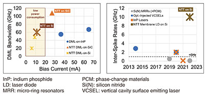
Fig. 1. Recent records of 3-dB bandwidths of DMLs [5, 6, 9–11] (left) and spike-processing rates of integrated photonic spiking neurons [7, 8] (right).
2. Membrane distributed-reflector lasers with integrated optical feedback
Our membrane laser structure for lasers fabricated on SiO2/Si substrates is based on a distributed-reflector longitudinal design that includes a middle uniform-distributed feedback (DFB) section sandwiched with an 80-μm-long back distributed Bragg reflector (DBR) mirror (DBR-r) and 200-μm-long front DBR mirror (DBR-ƒ). In this structure, the DBR-r is used to filter one of the two DFB modes for single-mode operation [12], and the DBR-ƒ is used to generate optical feedback and side-modes for enacting photon-photon dynamics [5, 6, 9–11] (see Fig. 2). Very low operating-power consumption was achieved with our heterogenous membrane III-V on Si technology, which uses a thin-film (<350-nm thick) III-V layer on a low-refractive index SiO2/Si substrate with a similar low-refractive index SiO2/silicon oxide (SiOx) overcladding. This structure enables very strong transverse optical confinement, which leads to both low operating power and high-speed dynamics. Other advantages include cost reduction by using large Si wafers and mature processes, co-integration capabilities with Si photonics and other integrated photonic platforms, and coupling to fibers via SiOx-based spot-size converters.
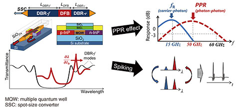
Fig. 2. Membrane distributed-reflector laser with integrated optical feedback [5–11].
3. Photon-photon resonance for short-reach communication links
Although our previously developed membrane DMLs could achieve high (~20 GHz) bandwidths with sub-pJ/bit energy consumptions [12], there is an inherent trade-off between further DML bandwidth improvement and power consumption since the relaxation oscillation frequency (ƒR) is proportional to the square-root of the bias current (Ib) above a threshold (Ith), i.e., ƒR ∝ (Ib – Ith)1/2. This limitation can be alleviated by introducing a photon-photon resonance (PPR) at high frequencies (see Fig. 2) on the basis of the optical-feedback-generated side-modes.
By using the PPR effect, we could effectively triple the bandwidths of the membrane DML-on-Si reaching ~60 GHz [5] while maintaining the same power consumption. This enabled us to achieve 112-Gbit/s short-reach transmissions for datacenter applications [5, 6] (see Fig. 3), and the first 400-Gbit/s-class link using a single >100-GHz-bandwidth DML-on-SiC [10]. We also demonstrated the ability to use the PPR effect at operating temperatures of 50℃ and above, which enabled us to sustain >100-Gbit/s operation for short-reach links using a membrane DML-on-Si at 50℃ [5, 6], and more than 100-GBaud modulations under uncooled (85℃) conditions using a membrane DML-on-SiC [11].
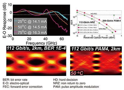
Fig. 3. Transmission performance of membrane DML-on-Si [5, 6].
4. Spiking membrane laser neurons
One of the most promising neuromorphic computing architectures in terms of energy-efficiency and scalability is the hardware implementation of spiking neural networks (SNNs) due to the unmatched noise-tolerance and event-driven capabilities of spike-information processing. In particular, integrated photonics hold great promise in offering high-bandwidth and scalable on-chip SNNs by taking advantage of the tens-of-GHz speeds offered by modern opto-electronics and the numerous parallelization capabilities of photonics. Nevertheless, most photonic implementations of spiking neurons to date have been limited by physical processes that operate on nanosecond time scales or slower, leading to spike-processing rates (i.e., the factor that ultimately defines the processing speed) of around the GHz level or less.
By using our membrane laser structure with integrated optical feedback, we were able to demonstrate ultrafast spiking behavior with clearly defined thresholds and spiking rates up to 10 GHz using 50-ps-long electrical pulses [7, 8] (see Fig. 4), overcoming previous speed limitations. This was achieved by taking advantage of the ultrafast photon-photon dynamics between two longitudinal modes (see Fig. 2). In such a case, a small input energy perturbation can temporarily excite a secondary longitudinal side-mode, which leads to power excitability of ultrashort (~ps long) output optical pulses, when the input energy perturbation exceeds an energy threshold. Moreover, our strong-confinement membrane-III-V-on-SiO2/Si structure ensured very low operating and threshold energies of ~pJ/spike and ~0.1 pJ/spike, respectively [7, 8].
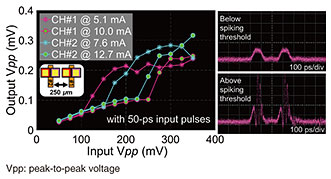
Fig. 4. Spiking effect in membrane lasers on Si [7, 8]. Note: oscilloscope data at ~240-ps inter-spike intervals are shown.
5. Summary and future plans
To meet the increasing demands on processing speeds of modern ICT and AI applications, while maintaining low operating energies for a sustainable and greener future within the IOWN project, we developed ultrafast and energy-efficient membrane distributed-reflector lasers on Si-based substrates with integrated optical feedback. With such lasers, we could achieve unprecedented DML bandwidths of ~60 GHz and spike-processing rates of 10 GHz with ~sub-pJ/bit and ~pJ/spike, respectively.
Future developments will focus on multi-channel DML transmitters for 800-Gbit/s systems and beyond by taking advantage of our previously developed techniques and technologies [13, 14]. We also plan to expand our spiking-membrane laser technology to multi-neuron SNN-PICs (photonic integrated circuits) and showcase their capabilities at solving practical computational tasks at unprecedented processing speeds.
References
| [1] |
International Energy Agency (IEA), “Data Centres and Data Transmission Networks,” 2022.
https://www.iea.org/reports/data-centres-and-data-transmission-networks |
| [2] |
N. C. Thompson, K. Greenewald, K. Lee, and G. F. Manso, “Deep Learning’s Diminishing Returns: The Cost of Improvement Is Becoming Unsustainable,” IEEE Spectrum, Vol. 58, No. 10, pp. 50–55, 2021.
https://spectrum.ieee.org/deep-learning-computational-cost |
| [3] |
NTT Corporation, “NTT Technology Report for Smart World 2022,” 2022.
https://www.rd.ntt/e/download/NTT_TRFSW_2022_E.pdf |
| [4] |
T. Sakamoto, N. Sato, and T. Segawa, “Photonics-electronics Convergence Technologies for Disaggregated Computing,” NTT Technical Review, Vol. 19, No. 7, pp. 58–64, 2021.
https://www.ntt-review.jp/archive/ntttechnical.php?contents=ntr202107fa8.html |
| [5] |
N.-P. Diamantopoulos, T. Fujii, S. Yamaoka, H. Nishi, K. Takeda, T. Tsuchizawa, T. Segawa, T. Kakitsuka, and S. Matsuo, “60 GHz Bandwidth Directly Modulated Membrane III-V Lasers on SiO2/Si,” Journal of Lightwave Technology, Vol. 40, No. 10, pp. 3299–3306, 2022.
https://doi.org/10.1109/JLT.2022.3153648 |
| [6] |
N.-P. Diamantopoulos, S. Yamaoka, T. Fujii, H. Nishi, K. Takeda, T. Tsuchizawa, T. Kakitsuka, and S. Matsuo, “47.5 GHz Membrane-III-V-on-Si Directly Modulated Laser for Sub-pJ/bit 100-Gbps Transmission,” Photonics, Vol. 8, No. 2, Article no. 31, 2021.
https://doi.org/10.3390/photonics8020031 |
| [7] |
N.-P. Diamantopoulos, S. Yamaoka, T. Fujii, H. Nishi, T. Segawa, and S. Matsuo, “Ultrafast Spiking Membrane III-V Laser Neuron on Si,” Proc. of 2022 European Conference on Optical Communication (ECOC 2022), paper Mo3G.2, Basel, Switzerland, Sept. 2022.
https://opg.optica.org/abstract.cfm?uri=ECEOC-2022-Mo3G.2 |
| [8] |
N.-P. Diamantopoulos, S. Yamaoka, T. Fujii, H. Nishi, T. Segawa, and S. Matsuo, “Stability of Spiking Effect in Membrane Laser Neurons on Si Utilizing Optical Feedback,” Proc. of 28th International Semiconductor Laser Conference (ISLC 2022), paper WC-02, Matsue, Japan, Oct. 2022.
https://doi.org/10.23919/ISLC52947.2022.9943397 |
| [9] |
S. Yamaoka, N.-P. Diamantopoulos, H. Nishi, R. Nakao, T. Fujii, K. Takeda, T. Hiraki, T. Tsurugaya, S. Kanazawa, H. Tanobe, T. Kakitsuka, T. Tsuchizawa, F. Koyama, and S. Matsuo, “Directly Modulated Membrane Lasers with 108 GHz Bandwidth on a High-thermal-conductivity Silicon Carbide Substrate,” Nature Photonics, Vol. 15, pp. 28–35, 2021.
https://doi.org/10.1038/s41566-020-00700-y |
| [10] |
N.-P. Diamantopoulos, H. Yamazaki, S. Yamaoka, M. Nagatani, H. Nishi, H. Tanobe, R. Nakao, T. Fujii, K. Takeda, T. Kakitsuka, H. Wakita, M. Ida, H. Nosaka, F. Koyama, Y. Miyamoto, and S. Matsuo, “>100-GHz Bandwidth Directly-modulated Lasers and Adaptive Entropy Loading for Energy-efficient >300-Gbps/λ IM/DD Systems,” Journal of Lightwave Technology, Vol. 39, No. 3, pp. 771–778, 2021.
https://doi.org/10.1109/JLT.2020.3021727 |
| [11] |
S. Yamaoka, N.-P. Diamantopoulos, H. Nishi, T. Fujii, K. Takeda, T. Hiraki, S. Kanazawa, T. Kakitsuka, and S. Matsuo, “Uncooled 100-GBaud Directly Modulated Membrane Lasers on SiC Substrate,” Journal of Lightwave Technology, 2023.
https://doi.org/10.1109/JLT.2023.3239614 |
| [12] |
T. Fujii, K. Takeda, N.-P. Diamantopoulos, E. Kanno, K. Hasebe, H. Nishi, R. Nakao, T. Kakitsuka, and S. Matsuo, “Heterogeneously Integrated Membrane Lasers on Si Substrate for Low Operating Energy Optical Links,” IEEE Journal of Selected Topics in Quantum Electronics, Vol. 24, No. 1, Article no. 1500408, 2018.
https://doi.org/10.1109/JSTQE.2017.2778510 |
| [13] |
T. Fujii, K. Takeda, H. Nishi, N.-P. Diamantopoulos, T. Sato, T. Kakitsuka, T. Tsuchizawa, and S. Matsuo, “Multiwavelength Membrane Laser Array Using Selective Area Growth on Directly Bonded InP on SiO2/Si,” Optica, Vol. 7, No. 7, pp. 838–846, 2020.
https://doi.org/10.1364/OPTICA.391700 |
| [14] |
H. Nishi, T. Fujii, N.-P. Diamantopoulos, K. Takeda, E. Kanno, T. Kakitsuka, T. Tsuchizawa, H. Fukuda, and S. Matsuo, “Integration of Eight-channel Directly Modulated Membrane-laser Array and SiN AWG Multiplexer on Si,” Journal of Lightwave Technology, Vol. 37, No. 2, pp. 266–273, 2019.
https://doi.org/10.1109/JLT.2018.2873742 |
 |
- Nikolaos-Panteleimon Diamantopoulos
- Research Scientist (Lead), Materials and Devices Laboratory, NTT Device Technology Laboratories.
He received a B.Sc. from University of Peloponnese, Tripoli, Greece in 2009, two M.Sc. degrees from Aston University, Birmingham, UK and Scuola Superiore Sant’Anna Pisa (SSSUP), Pisa, Italy in 2012 under the joint-masters Erasmus Mundus program, and a Ph.D. from Osaka University, Japan in 2016. From 2011 to 2016, he was involved in several EU-funded R&D projects at the Athens Information Technology (AIT) research center, Athens, Greece. Since 2016 he has been with NTT Device Technology Labs, where he conducts research on integrated photonics, optical communications, digital signal processing, neuromorphic computing systems, space-division multiplexing, and semiconductor lasers. He is a senior member of the Institute of Electrical and Electronics Engineers (IEEE) and Optica.
|
 |
- Suguru Yamaoka
- Researcher, Materials and Devices Laboratory, NTT Device Technology Laboratories.
He received a B.E., M.E., and Ph.D. in applied physics from Osaka City University in 2015, 2017, and 2021. In 2017, he joined NTT Device Technology Labs. His research interests include high-speed and low-power-consumption directly modulated semiconductor lasers. He is a member of the Institute of Electronics, Information and Communication Engineers (IEICE) and the Japan Society of Applied Physics (JSAP).
|
 |
- Takuro Fujii
- Research Scientist (Lead), Materials and Devices Laboratory, NTT Device Technology Laboratories and NTT Nanophotonics Center.
He received a B.E. and M.E. in system design engineering from Keio University, Kanagawa, in 2010 and 2012. In 2012, he joined NTT Photonics Laboratories, where he has been researching metalorganic vapor phase epitaxy growth of III-V semiconductors and the development of III-V semiconductors and III-V semiconductor lasers on Si for photonic integrated circuits. He was the recipient of the Young Scientist Presentation Award from JSAP in 2014. He is a member of IEICE, JSAP, and IEEE.
|
 |
- Shinji Matsuo
- Senior Distinguished Researcher, Materials and Devices Laboratory, NTT Device Technology Laboratories and NTT Nanophotonics Center.
He received a B.E. and M.E. in electrical engineering from Hiroshima University in 1986 and 1988, and Ph.D. in electronics and applied physics from Tokyo Institute of Technology in 2008. In 1988, he joined NTT Optoelectronics Laboratories, where he researched photonic functional devices using MQW pin modulators and VCSELs. In 1997, he researched optical networks using wavelength division multiplexing technologies at NTT Network Innovation Laboratories. Since 2000, he has been researching high-speed tunable optical filters and lasers at NTT Photonics Laboratories and NTT Device Technology Laboratories. He is a member of JSAP and IEICE, and a fellow of IEEE and Optica.
|
↑ TOP
|


